Method and apparatus for laser trimming of resistors using ultrafast laser pulse from ultrafast laser oscillator operating in picosecond and femtosecond pulse widths

Inactive Publication Date: 2006-02-23
LASERFACTURING
View PDF22 Cites 76 Cited by
  • Summary
  • Abstract
  • Description
  • Claims
  • Application Information

AI Technical Summary

Benefits of technology

[0058] In another aspect of present invention, it is possible to producing feature size of less than one twentieth of the focused spot size of the ultrafast pulse laser beam. This can be achieved by precisely controlling the laser threshold fluence slightly above the ablation threshold of the material and by precisely controlling the number of pulse and the duration between the pulses (minimizing or eliminating the cumulative heating effect) using the pulse modulation means disclosed in this invention. In addition the stability of the laser pulse from the ultrafast laser oscillator plays a vital role in machining feature of desired size with repeatability and precision.
[0059] In another aspect of the present invention, the pulse energy plays a vital role in micro and nano processing with high quality. The pulse energy required to ablate a feature depends on the depth of ablation, repeatability of feature size required and the feature quality. The maximum depth that can be generated for a given focused spot size of the laser beam depends on the pulse energy. As the ablated feature becomes deeper it is difficult to remove the ablated material from the hole and hence the ablated material absorbs the energy of the subsequent pulse. Also the uncertainty in the feature size obtained will depend on the number of pulse required to ablate the required feature. Due to the topography generated and debris deposited in the crater by the ablation of the first pulse the absorption of the successive pulse is different due to the defects generated in the previous pulse, scattering of the laser beam etc. Due to the above mechanism the ablation threshold of the successive pulse may be vary. The uncertainly in the diameter of ablated feature increases with increase in the number of pulse. Also, higher pulse energy generates sufficient pressure for ejecting the debris out of the carter and hence the successive pulse will interact with the fresh substrate. This results in improved top surface and inner wall quality of the ablated feature. Hence it is advantageous to higher pulse energy and lower number of pulse to ablate a required feature.
[0060] In another aspect of the invention, the effect of wavelength on the cutting efficiency and stability of micron and nano processing using laser pulse from ultrafast laser oscillator is disclosed. In ultrafast laser processing the wavelength of the laser beam does not have a major impact on the threshold fluence of the materi

Problems solved by technology

There is negligible thermal conduction beyond the ablated region resulting in negligible stress or shock to surrounding material.
The system is very unstable in terms of laser power and laser pointing stability.
The average laser power is very low to meet the industrial throughput The Amplified femtosecond laser technology is very expensive, which will increase the manufacturing cost considerably.
The down time of the system is high to the complexity of the laser system Large floor space of the laser system Very poor feature size and depth controllability due to laser power fluctuation Experiences and trained profession are required for the maintenance of the system
The resultant amplified pulse has repletion rate ranging from 500 Hz to 300 KHz of average power 1 to 10 W. Although amplified picosecond laser is simple and compact in comparison to amplified femtosecond laser but has the following limitations, which prevents it from being used for high volume manufacturing applications in industry, The Amplified picosecond laser also more stable than an amplified femtosecond laser system, it is still unstable in terms of laser power and laser pointing stability to meet the needs for industrial high volume manufacturing applications.
The Amplified picosecond femtosecond laser technology also cheaper than amplified femtosecond laser system it is still expensive, which will increase the manufacturing cost considerably.
Very poor feature size and depth controllability due to laser power fluctuation The down time of the system is high.
But due to short time gap between the successive pulses, there is a considerable degrade in the machining quality, which may be explained as below.
The enhanced surface temperature of the ablation front will cause over heating and deteriorate the quality of ablation.
In the case of via drilling application, such over heating deteriorate the geometry of via, causing barrel at the bottom of the hole.
Although the U.S. patent shows a general application of using ultrafast pulse laser directly for micro machining, due to cumulative heating effect there is temperature rise around the focal area and hence there will be considerable heat accumulation surrounding the ablated feature.
Following are some of the drawbacks due to the effect Difficult to be used for nanoscale maching application due to heat accum

Method used


Image

  • Method and apparatus for laser trimming of resistors using ultrafast laser pulse from ultrafast laser oscillator operating in picosecond and femtosecond pulse widths
  • Method and apparatus for laser trimming of resistors using ultrafast laser pulse from ultrafast laser oscillator operating in picosecond and femtosecond pulse widths
  • Method and apparatus for laser trimming of resistors using ultrafast laser pulse from ultrafast laser oscillator operating in picosecond and femtosecond pulse widths

Examples


Example

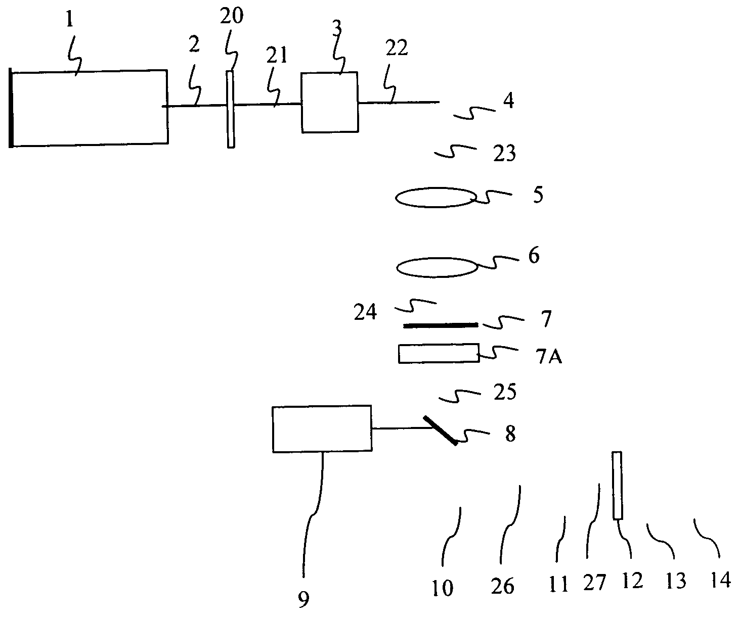
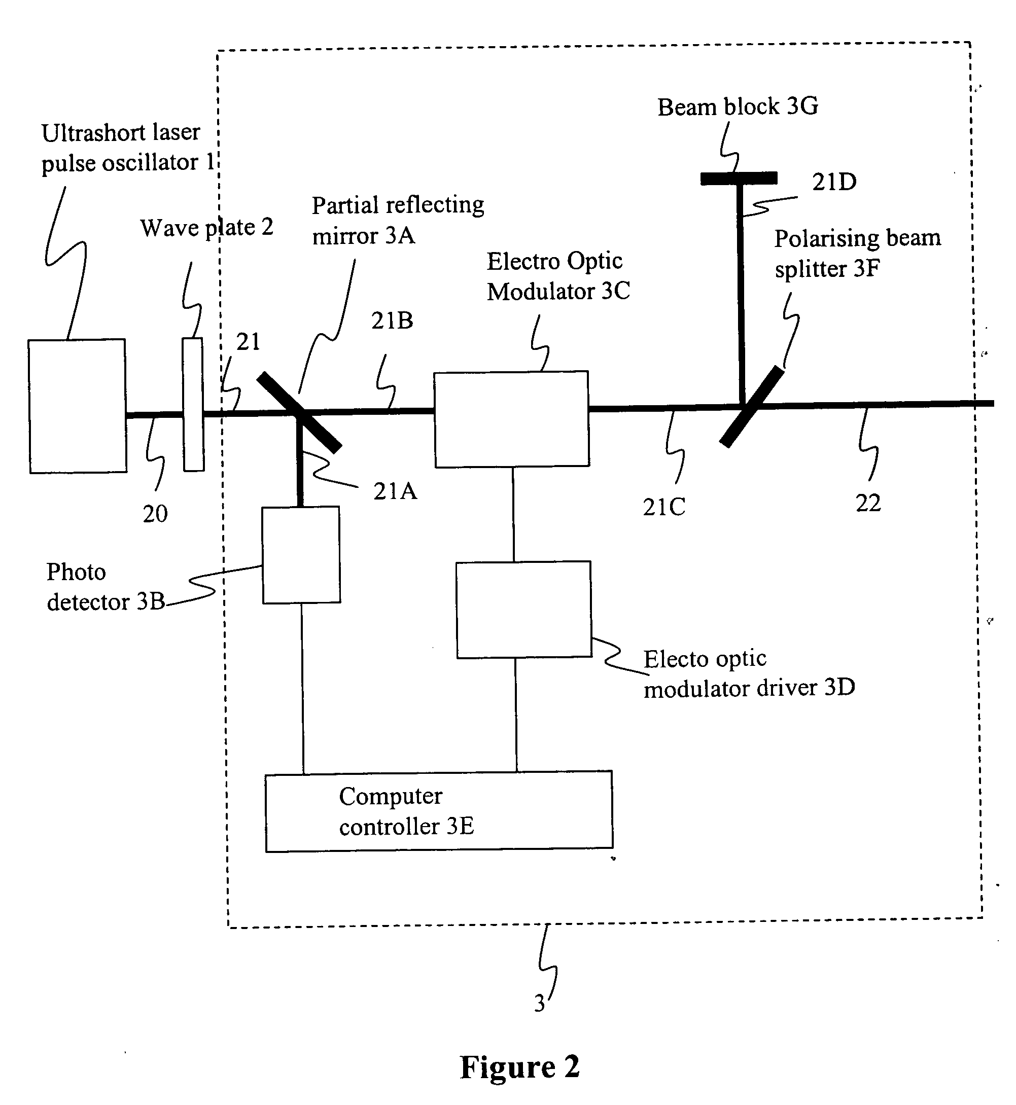
DETAILED DESCRIPTION OF THE DRAWINGS

[0089] The object of the present invention is to provide improved method and apparatus for micro / nano machining and to ameliorate the aforesaid deficiencies of the prior art by using ultrafast pulse generated directly from the laser oscillator. The laser oscillators are mode locked diode pumped solid state laser system, which is stable and compact. The pulse laser beam having a pulse width of 1 fs to 100 ps of repletion rate from 1 MHz to 400 MHz is controlled by electro optic modulator or acousto optic modulator.

[0090] The modulated pulse is expanded to required beam diameter by using combination of positive and negative lens to act as a telescope. Varying the diameter of the laser beam the focused laser spot size can be varied. The pulsed laser beam scanned by a 2 axis galvanometer scanner to scan the pulse laser beam on the surface of the work piece in a predetermined pattern. The scanning beam can be focused on a work piece using a focusing ...


PUM

PropertyMeasurementUnit
Lengthaaaaaaaaaa
Fractionaaaaaaaaaa
Fractionaaaaaaaaaa

Abstract

The present invention relates to a method and apparatus for laser trimming of resistors in semiconductor applications using ultrafast laser pulse from diode pumped or CW pumped solid state mode locked ultrafast pulse laser oscillator without amplification. The invention disclosed has a means to avoid/reduce the cumulative heating effect to avoid machine quality degrading in multi shot ablation. The disclosed invention provides a cost effective and stable system for high volume manufacturing application. The disclosed invention is used for thick and thin film trimming. Ultrafast laser oscillator can be a called as femtosecond laser oscillator or a picosecond laser oscillator depending on the pulse with of the laser beam generated.

Description

[0001] The present application claims the benefit of Provisional Application No. 60 / 601,653, filed on Aug. 16, 2005, the entire contents of which is incorporated herein by reference.TECHNICAL FIELD OF THE INVENTION [0002] The present invention relates to a method and apparatus for laser trimming of resistors in semiconductor applications using ultrafast laser pulse, and more specifically it relates to using diode pumped or CW pumped solid state mode locked ultrafast pulse laser oscillator without amplification. BACKGROUND OF THE INVENTION [0003] Amplified short pulse laser of pulse width 100 picosecond to 10 femtosecond are being used in general applications to overcome the problem of long pulse laser. The advantage of short pulse lasers in comparison to long pulse laser are [0004] Since the duration of short pulse laser is shorter than the heat dissipation time, the energy does not have the time to diffuse away and hence there is minimal or no heat affected zone and micro cracks. [...

Claims


Application Information

Patent Timeline
IPC IPC(8): H01S3/10
CPCH01C17/242B23K26/0635B23K26/0624H01S3/0085H01S3/1106
Inventor DESHI, TAN
Owner LASERFACTURING
Why Eureka
Try Eureka