Bipolar differential to single ended transfer circuit with gain boost

a transfer circuit and gain boost technology, applied in the field of differential to single-ended signal transfer circuit improvement, can solve the problems of affecting the affecting the ac performance and stability of the op amp, and imbalanced differential input stages, so as to increase the input impedance increase and reduce the input current of the transfer circuit.

Active Publication Date: 2006-03-02
TEXAS INSTR INC
View PDF3 Cites 13 Cited by
  • Summary
  • Abstract
  • Description
  • Claims
  • Application Information

AI Technical Summary

Benefits of technology

[0013] In accordance with the present invention, a two-stage bipolar rail-to-rail operational amplifier (op amp) is provided including a differential to single-ended signal transfer circuit that allows increased open loop gain and improved AC performance, while reducing operating power supply voltage requirements. The differential to single-ended transfer circuit provides highly accurate base current cancellation without lengthening the signal path within the circuit.
[0015] As a result, the operating points of the first and second transistors are substantially the same. Further, the respective base currents of the first and second transistors substantially cancel one another, thereby allowing the input current of the transfer circuit to be reduced while increasing the input impedance of the circuit. Such base current cancellation is obtained without increasing the length of the signal path within the transfer circuit. Further, the increased input impedance of the transfer circuit is achieved while reducing the parasitic conductance associated with the high impedance node.
[0016] By providing high input impedance with reduced parasitic conductance, and by implementing base current cancellation off of the signal path, the presently disclosed differential to single-ended transfer circuit may be incorporated into a two-stage bipolar rail-to-rail op amp to obtain increased open loop gain and improved AC performance.

Problems solved by technology

One drawback of the transfer circuits 100 and 100a employing current mirrors with tracking feedback is that the input conductance associated with the single-ended second stage can cause the differential input stage to become imbalanced, thereby degrading the open loop gain of the two-stage bipolar op amp.
However, because this approach increases the number of sub-stages within the second stage, the AC performance and the stability of the op amp may be adversely affected.
However, the base current cancellation technique of FIG. 2 also has drawbacks.
For example, due to the different collector-emitter voltages of the transistors Q1-Q2 of the transfer circuit 200, the betas of the transistors Q1-Q2 may be different, thereby causing an error in the base current cancellation.
Further, the transfer circuit 200 is normally not suited for use with low power supply voltages due to the additional voltage drop across the transistor Q2.
Moreover, the inverting and non-inverting inputs INn and INp of the transfer circuit 200 may be imbalanced, thereby exacerbating the base current cancellation error.
In addition, in the event a boosted stage configuration of the transfer circuit 200 is employed (see, e.g., the transfer circuit 300 of FIG. 3), the additional phase shift created by the transistor Q2 within the local feedback loop of the transfer circuit 300 may degrade the AC performance and adversely affect the stability of the op amp.

Method used


Image

  • Bipolar differential to single ended transfer circuit with gain boost
  • Bipolar differential to single ended transfer circuit with gain boost
  • Bipolar differential to single ended transfer circuit with gain boost

Examples


embodiment 500

[0036]FIG. 5 depicts an alternative embodiment 500 of the differential to single-ended signal transfer circuit 400 (see FIG. 4). Like the transfer circuit 400, the transfer circuit 500 comprises the current mirror 401, the base current cancellation circuit 403, and the output buffer 405. The transfer circuit 500 further includes transistors Q3 and Q4, and a fourth current source I4. In the illustrated embodiment, the transistors Q3 and Q4 comprise respective PNP-type bipolar junction transistors (BJTs), and the current source I4 is implemented using the same bipolar IC technology as the BJTs Q1-Q4.

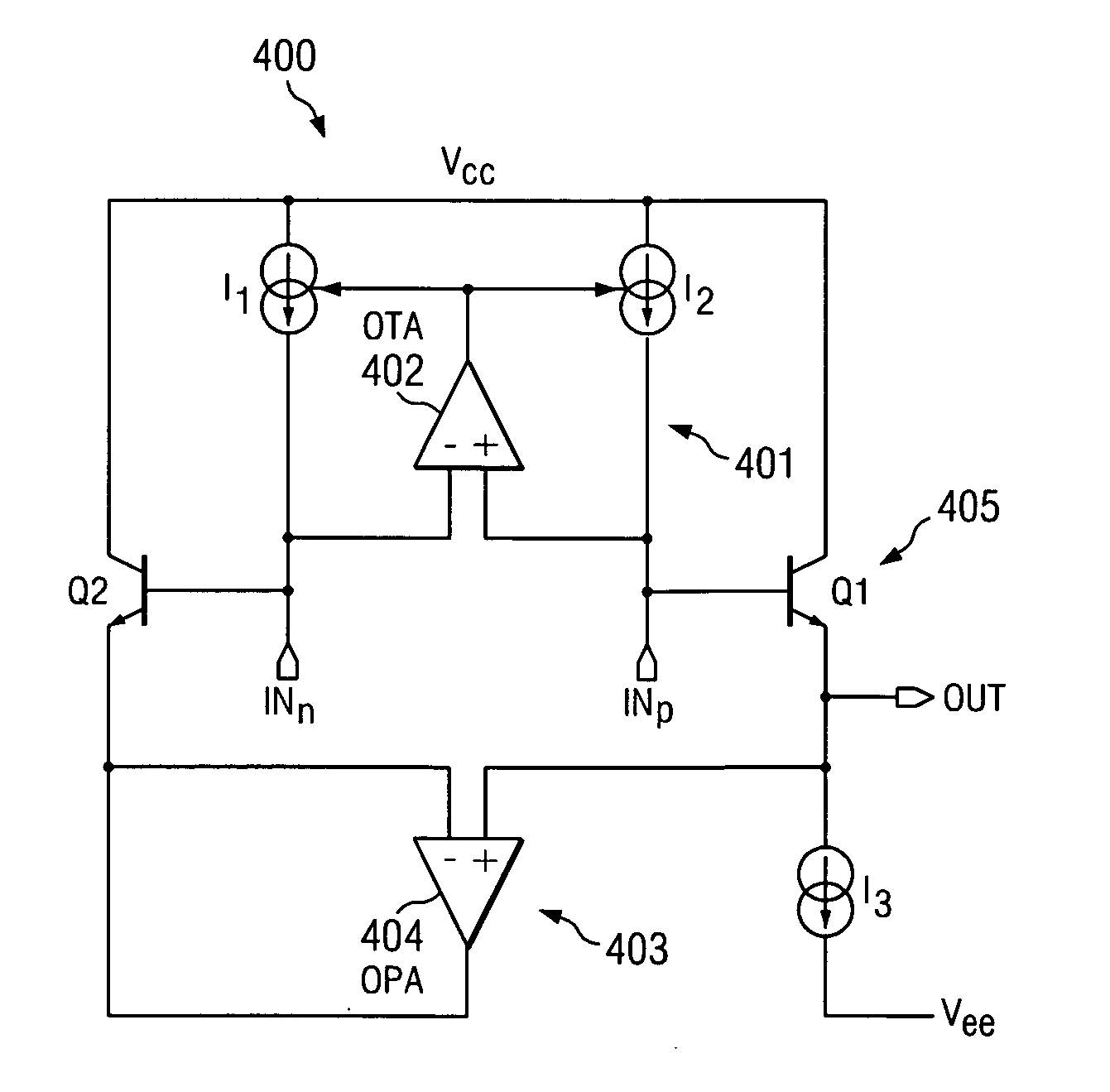
[0037] Specifically, the transistor Q3 and the current source I4 are configured to boost the current gain of the output buffer 405 including the transistor Q1. Further, because the addition of the transistor Q3 and the current source I4 may change the collector voltage of the transistor Q1, the diode-connected transistor Q4 is added to the transfer circuit 500 and configured to assure that...

embodiment 600

[0038]FIG. 6 depicts an alternative embodiment 600 of the differential to single-ended signal transfer circuit 500 (see FIG. 5). Like the transfer circuit 500, the transfer circuit 600 comprises the current mirror 401, the base current cancellation circuit 403, the output buffer 405, the transistor Q3, and the current source I4. However, in place of the diode-connected transistor Q4 included in the transfer circuit 500, the transfer circuit 600 includes a third operational amplifier (OPA) 406 coupled between the respective collectors of the transistors Q1-Q2 as a voltage follower, thereby assuring that the collector voltage of the transistor Q2 is substantially equal to the collector voltage of the transistor Q1.

[0039]FIG. 7 depicts a detailed view 700 of the transfer circuit 500 (see FIG. 5). In the illustrated embodiment, a first circuit portion 702 corresponds to the OTA 402 (see FIGS. 4-5), and a second circuit portion 704 corresponds to the OPA 404 (see FIGS. 4-5). Specifically...

embodiment 800

[0042]FIG. 8 depicts an alternative embodiment 800 of the differential to single-ended signal transfer circuit 500 (see FIG. 5). Like the transfer circuit 500, the transfer circuit 800 comprises the OTA 402, the OPA 404, and the output buffer 405. The transfer circuit 800 further comprises a differential input stage 830, a folded cascode section 832, and a class-A output stage 820 coupled to the output buffer 405. The differential input stage 830 includes PNP-type BJTs Q1001 and Q1002, and a current source I1000. The folded cascode section 832 includes NPN-type BJTs Q1003 and Q1004 biased by a voltage source Vbias, and emitter degeneration resistors R1-R2 coupled between the transistors 1003-1004 and the supply voltage Vee, respectively. The class-A output stage 820 includes an emitter-follower transistor Q100, and a current source I101.


PUM


Abstract

A differential to single-ended signal transfer circuit that allows increased gain and improved AC performance while reducing power supply voltage requirements. The transfer circuit includes a first operational transconductance amplifier (OTA), a second operational amplifier (OPA), first and second controlled current sources, a third current source, and first and second bipolar junction transistors. The inverting and non-inverting inputs of the transfer circuit are provided at the inverting input and the non-inverting input, respectively, of the OTA, which is coupled to the first and second controlled current sources to form a current mirror with tracking feedback. The output voltage of the transfer circuit is provided at the emitter of the first transistor, the base of which is connected to the non-inverting input INp. The first transistor is coupled to the third current source in an emitter follower configuration to provide both current gain and impedance matching. The base of the second transistor is connected to the inverting input of the transfer circuit. The OPA is coupled between the respective emitters of the first and second transistors in a voltage follower configuration.

Description

CROSS REFERENCE TO RELATED APPLICATIONS [0001] N / A STATEMENT REGARDING FEDERALLY SPONSORED RESEARCH OR DEVELOPMENT [0002] N / A BACKGROUND OF THE INVENTION [0003] The present application relates generally to improvements in differential to single-ended signal transfer circuits, and more specifically to techniques for increasing the open loop gain, for improving the AC performance, and for reducing the power supply voltage requirements of operational amplifiers including such transfer circuits. [0004] Two-stage bipolar operational amplifiers are known that include a differential input stage and a single-ended second stage. For example, a conventional two-stage bipolar operational amplifier (op amp) may include a differential input stage, a differential to single-ended signal transfer circuit, a single-ended second stage, and an output buffer. In the conventional two-stage bipolar op amp, the differential to single-ended transfer circuit may comprise a current mirror, the single-ended s...

Claims


Application Information

Patent Timeline
Patent Type & Authority Applications(United States)
IPC IPC(8): H03F3/45
CPCH03F3/3069H03F2203/45288H03F3/45085
Inventor ALENIN, SERGEY
Owner TEXAS INSTR INC
Why Eureka
Try Eureka