Pixel and organic light emitting display comprising the same, and driving method thereof
- Summary
- Abstract
- Description
- Claims
- Application Information
AI Technical Summary
Problems solved by technology
Method used
Image

Examples
first embodiment
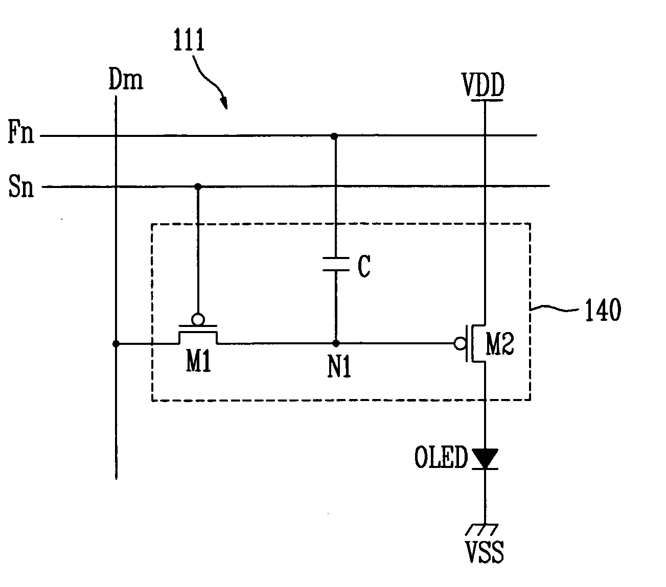
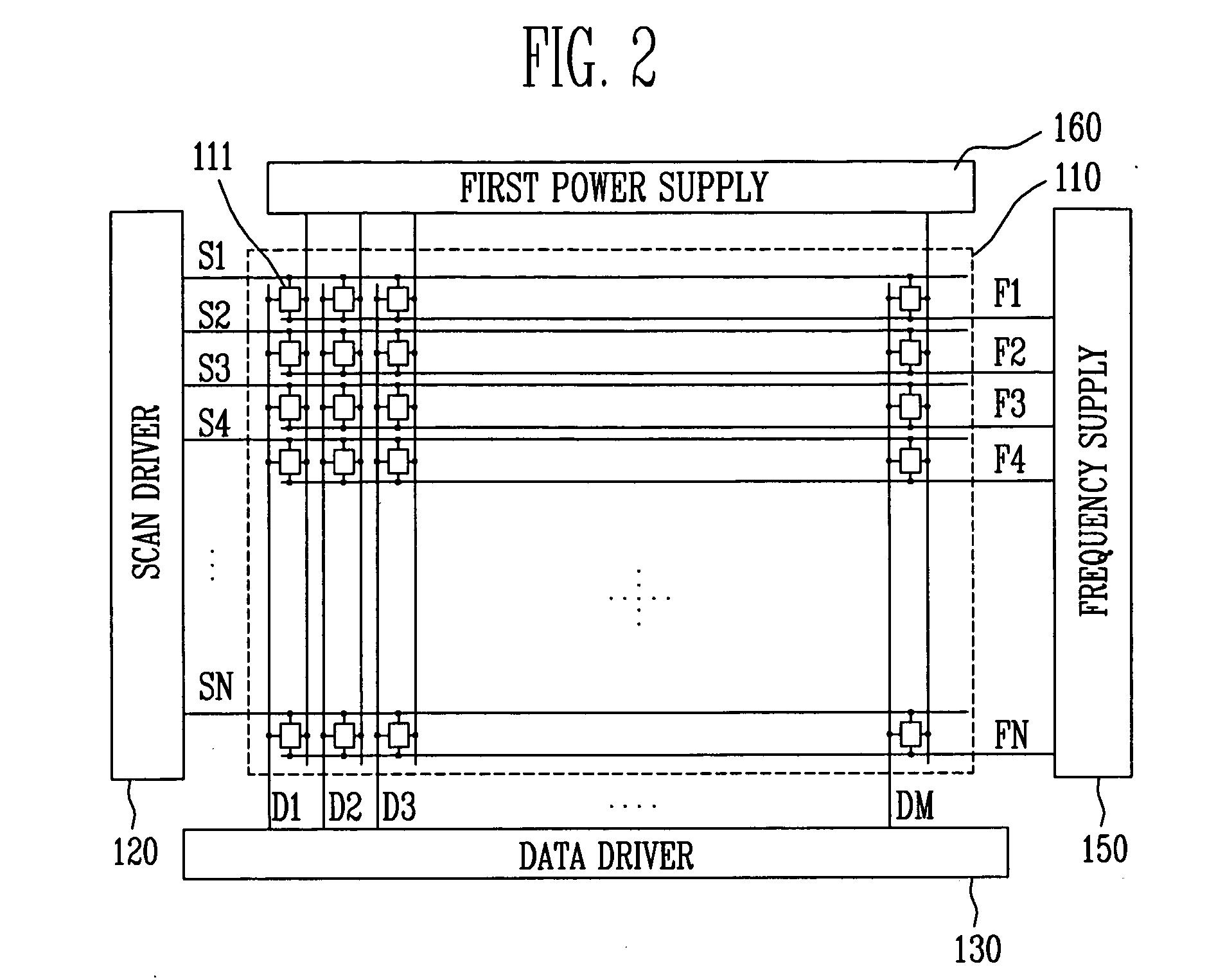
[0041]FIG. 2 illustrates an organic light emitting display comprising a pixel according to the invention.
[0042] Referring to FIG. 2, the illustrated pixel comprises a pixel portion 110, a scan driver 120, a data driver 130, a first power supply 160, and a frequency supply 150.
[0043] The pixel portion 110 comprises a plurality of pixels 111, wherein the pixels 11 are defined by a plurality of scan lines S1 through SN, a plurality of data lines D1 through DM, a plurality of pixel power source lines, and a plurality of frequency supplying lines F1 through FN. In one embodiment, the plurality of pixels 111 receives second power from a second power supply (not shown), wherein the second power is different from the first power.
[0044] The pixel 111 is selected when a scan signal is transmitted to the scan line S1 through SN, and emits light corresponding to a data signal transmitted to the data line DM and a frequency signal transmitted to the frequency supplying lines F1 through FN. Spe...
second embodiment
[0052]FIG. 4 is a control block diagram showing the frequency supply illustrated in FIG. 2. Referring to FIG. 4 in accordance with FIG. 2, the frequency supply 150 comprises a counter part 254, a shift register part 252, and a selector 256.
[0053] The counter part 254 is started by a count starting signal and generates a plurality of count output signals COS having different frequencies according to input clock signals (CLK), wherein the count output signals COS are supplied to the selector 256. In one embodiment, the count output signals COS generated by the counter 254 have different frequencies corresponding to the respective bits (or each sub-frame) among the i bit digital data signals.
[0054] Each shift register is configured to sequentially shift a starting signal synchronized with the scan signal, thereby supplying the shifted starting signal to the selector 256. Specifically, each shift register outputs a bit selection signal BSS to the selector 256. In one embodiment, each s...
third embodiment
[0056]FIG. 5 is a block diagram illustrating the frequency supply illustrated in FIG. 2. Referring to FIG. 5 in accordance with FIG. 2, the frequency supply 150 comprises a voltage controlled oscillator circuit 358, a shift register part 352, and a selector 356.
[0057] The voltage controlled oscillator circuit 358 comprises a plurality of voltage controlled oscillators. Each voltage controlled oscillator generates a plurality of different frequency signals VO based on different supply voltages, and supplies the frequency signals VO to the selector 356. Specifically, the voltage controlled oscillator circuit 358 generates a lower frequency signal VO as a bit among the digital data signals of i bits approaches the most significant bit, and supplies the frequency signal VO to the selector 356.
[0058] The shift register part 352 comprises a plurality of shift registers. Each shift register is configured to sequentially shift a voltage selection signal VSSS synchronized with the scan sign...
PUM
 Abstract
Description
Claims
Application Information
 - R&D Engineer
- R&D Manager
- IP Professional
- Industry Leading Data Capabilities
- Powerful AI technology
- Patent DNA Extraction
Browse by: Latest US Patents, China's latest patents, Technical Efficacy Thesaurus, Application Domain, Technology Topic.
© 2024 PatSnap. All rights reserved.Legal|Privacy policy|Modern Slavery Act Transparency Statement|Sitemap