
Semiconductor-insulator-semiconductor structure for high speed applications

a technology of semiconductor and semiconductor, applied in the direction of semiconductor/solid-state device details, instruments, semiconductor devices, etc., can solve the problems of severe retardation of the switching capability of modulators, and achieve the effect of reducing grain boundaries

Inactive Publication Date: 2006-03-23
HONEYWELL INT INC
View PDF72 Cites 30 Cited by
  • Summary
  • Abstract
  • Description
  • Claims
  • Application Information

AI Technical Summary

Benefits of technology

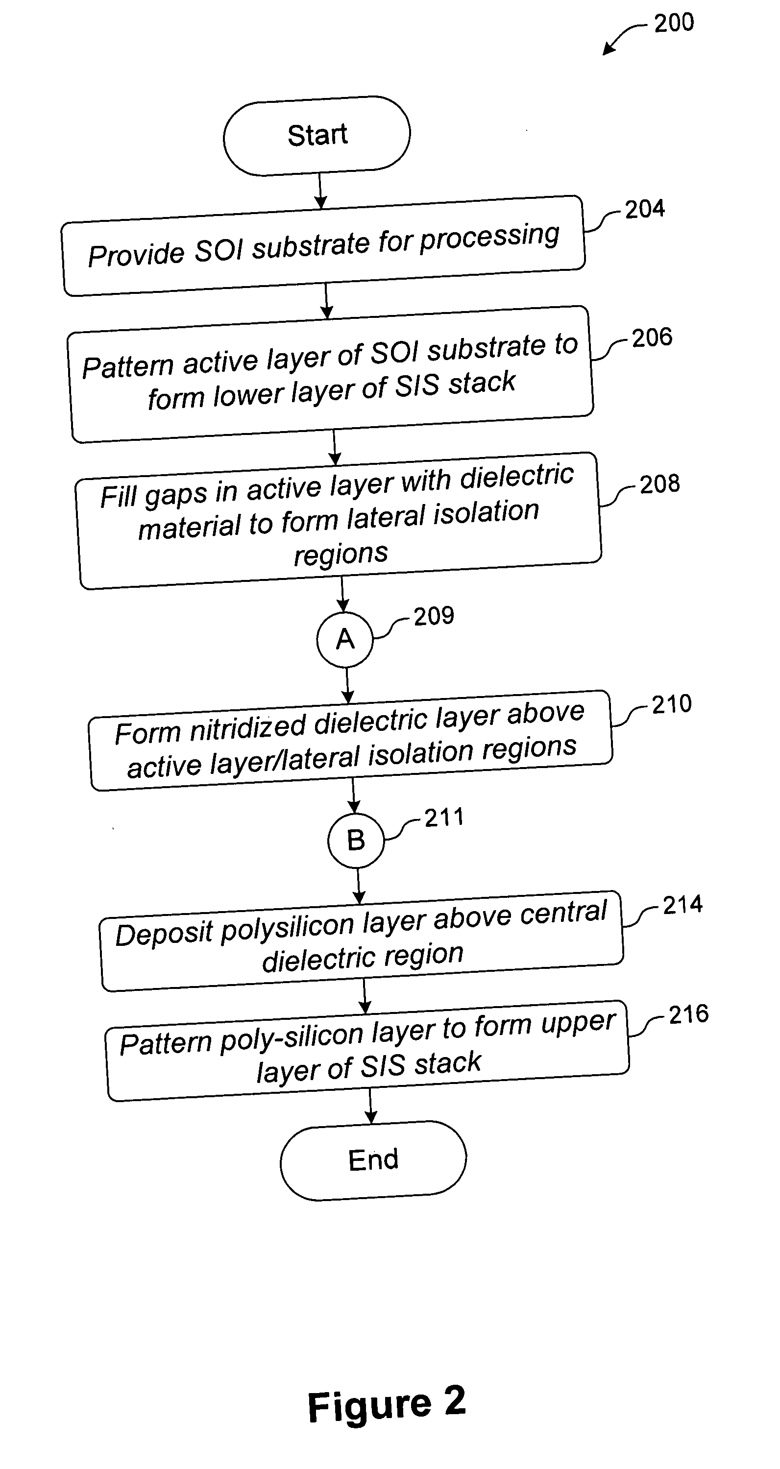
[0009] In another aspect, the invention relates to a method for creating an SIS device includes: providing an active semiconductor layer on an insulating substrate; etching portions of the active semiconductor layer to create a laterally isolated lower semiconductor layer; forming lateral isolation regions that laterally bound the lower semiconductor layer; forming a central dielectric region over a portion of the lower semiconductor layer, where the central dielectric region is nitridized; and forming an upper semiconductor layer that overlaps the central dielectric region. In one embodiment, the central dielectric region may be formed by thermally growing silicon dioxide in an atmosphere having a controlled flow of nitrogen such that the silicon dioxide is infused with nitrogen. In another embodiment, the central dielectric region may be formed by depositing a layer of silicon dioxide using a CVD process having a controlled flow rate of nitrogen, such that the silicon dioxide is infused with nitrogen. Additionally, the above method may include the step of infusing the central dielectric region with nitrogen using an implantation process. In another embodiment, the upper semiconductor layer may be poly-silicon and the above method may include annealing the device at a high temperature in order to reduce grain boundaries in the upper poly-silicon semiconductor layer.

Problems solved by technology

The result is a severe retardation of the switching capabilities of the modulator due to the formation of speed-limiting junctions within the Si layers.

Method used


Image

  • Semiconductor-insulator-semiconductor structure for high speed applications
  • Semiconductor-insulator-semiconductor structure for high speed applications
  • Semiconductor-insulator-semiconductor structure for high speed applications

Examples


Embodiment Construction

[0014] This invention relates to the improvement of diffusion profiles in semiconductor-insulator-semiconductor (SIS) stacks, specifically silicon-insulator-silicon stacks, which can be used in integrated capacitor-based electro-optic modulators. The central insulating layer of the SIS stack is infused with nitrogen, thereby helping to prevent the migration of dopants between semiconducting layers in the SIS stack. The reduction in the permeability of the insulating layer results in an optimized switching capability for any modulating device that includes the SIS stack.

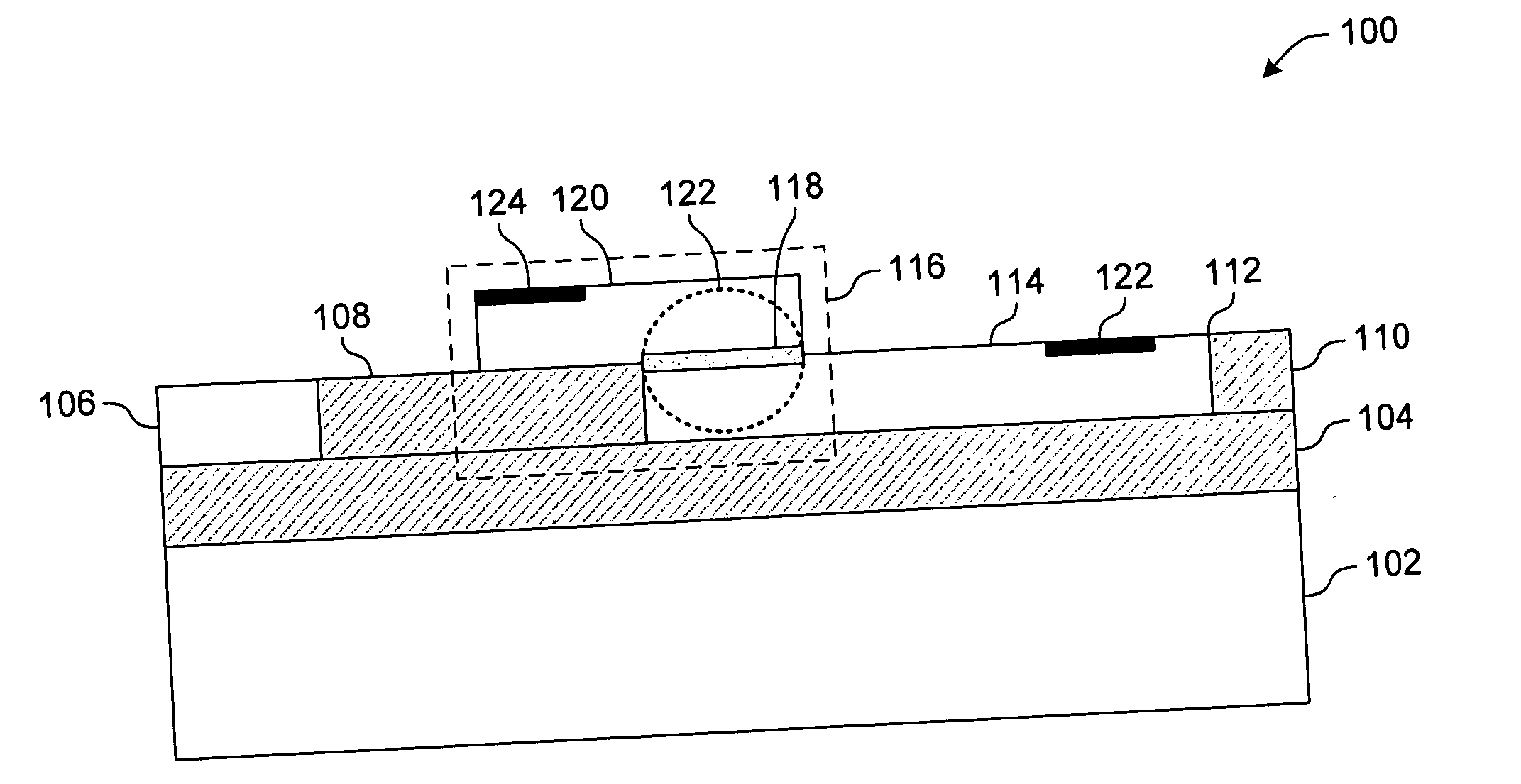
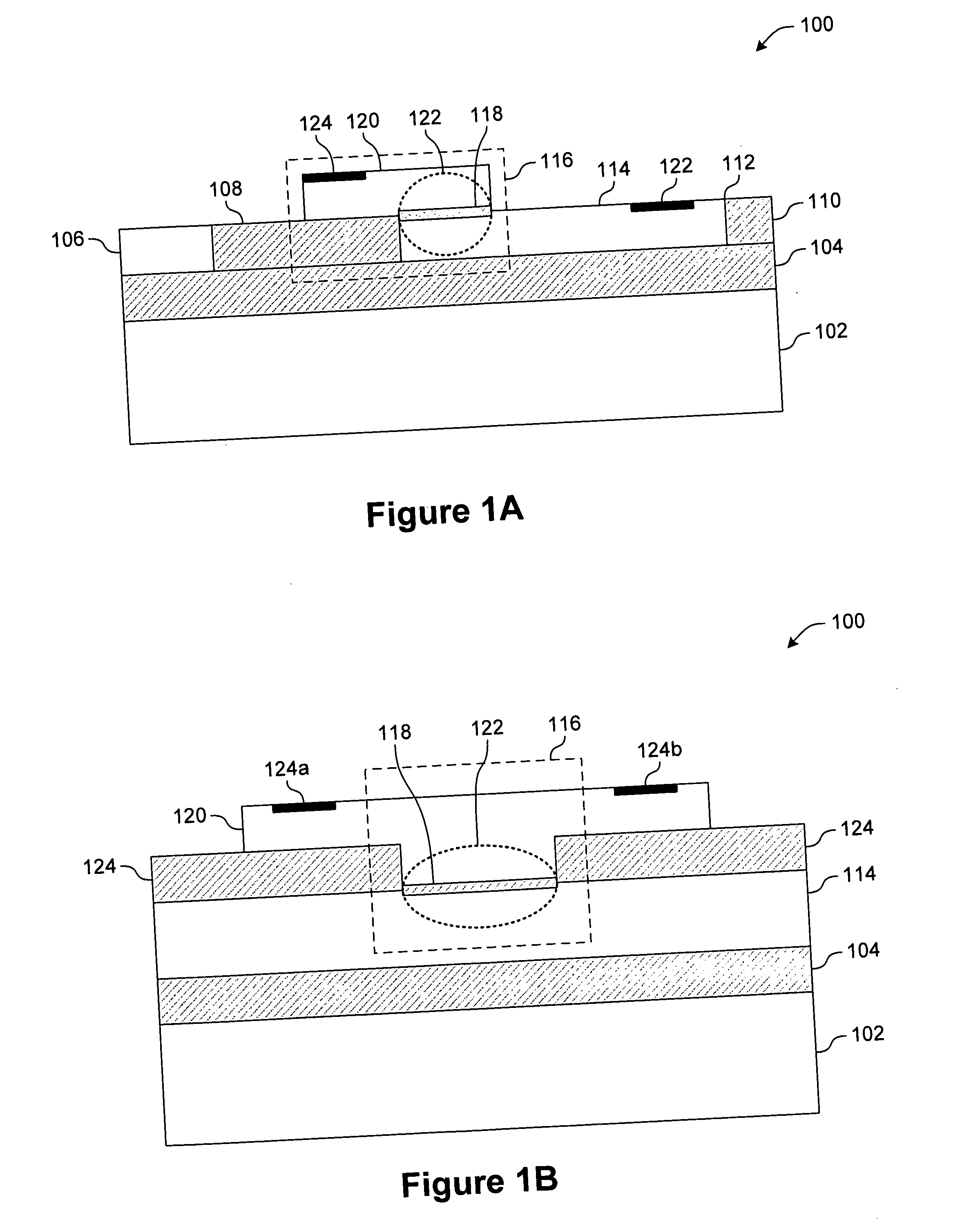
[0015]FIG. 1 provides two cross-sectional views of an optical modulator 100 that includes a semiconductor-insulator-semiconductor (SIS) device 116 with a nitridized central insulating layer 118, according to an embodiment. FIG. 2 illustrates a process diagram for creating the structure 100. The optical modulator 100 may be created by utilizing a silicon-on-insulator (SOI) substrate with the top (active) silicon subst...


PUM


Abstract

A semiconductor-insulator-semiconductor (SIS) device is presented along with a device for fabricating the same. The SIS device includes a lower semiconductor layer, an upper semiconductor layer, and a central insulating layer located between the overlapping portions of the lower semiconductor layer and the upper semiconductor layer. The central insulating layer is nitridized in order to make the layer less permeable to dopant species and to therefore minimize dopant cross-diffusion. Subsequently the switching characteristics of the SIS device are optimized when the SIS device is used as, for example, an integrated optical modulator.

Description

PRIORITY [0001] This application claims priority to and incorporates by reference the entirety of U.S. Provisional Application No. 60 / 611,210, “Semiconductor-Insulator-Semiconductor Structure for High Speed Applications,” filed on Sep. 17, 2004.BACKGROUND OF THE INVENTION [0002] 1. Field of the Invention [0003] The present invention relates to the field of semiconductor devices and, more especially, to semiconductor-insulator-semiconductor structures with improved doping profiles for high speed applications. [0004] 2. Description of the Related Art [0005] By definition, optical modulators are devices that can change the phase, intensity, polarization, direction, or some other characteristic of light. Modulation of any of these optical characteristics by a modulator can be advantageously used to load an optical stream with encoded data. Using an electro-optic modulator, electrical signals can be directly converted into optically encoded data. Such a device allows for information to b...

Claims


Application Information

Patent Timeline
Patent Type & Authority Applications(United States)
IPC IPC(8): H01L39/22
CPCG02F1/025
Inventor YUE, CHEISAN J.KEYSER, THOMAS
Owner HONEYWELL INT INC
Learn More