Thin film containing nanocrystal particles and method for preparing the same

a nanocrystal particle and nanocrystal technology, applied in the field of thin film containing nanocrystal particles and a method for preparing the same, can solve the problems of low deposition speed, non-uniform surface state of the thin film prepared thereby, and applicability to processing, so as to improve the crystallinity of the thin film and reduce grain boundaries

Active Publication Date: 2013-08-06
SAMSUNG ELECTRONICS CO LTD
View PDF9 Cites 10 Cited by
  • Summary
  • Abstract
  • Description
  • Claims
  • Application Information

AI Technical Summary

Benefits of technology

[0010]Therefore, the present invention has been made in view of the problems of the prior art. Thus, in an embodiment, a thin film containing nanocrystal particles is provided, in which the nanocrystal is used as a nucleus for crystal growth to reduce grain boundaries of the thin film, thereby improving the crystallinity of the thin film.
[0011]In another embodiment, a method for the preparation of a thin film containing nanocrystal particles is disclosed in which the nanocrystal is used as a nucleus for crystal growth to reduce grain boundaries of the thin film, thereby improving the crystallinity of the thin film.
[0012]In another embodiment, an electronic device comprising a thin film containing nanocrystal particles is provided in which the nanocrystal is used as a nucleus for crystal growth to reduce grain boundaries of the thin film, thereby improving the crystallinity of the thin film.

Problems solved by technology

However, this deposition method suffers from problems of low deposition speed and disadvantageous applicability to processing arising from the use of a chemical bath.
However, the ESAVD technique poses a problem in that the surface state of the thin films prepared thereby is non-uniform when compared to that of thin films prepared by spin coating.
Since the size of nanocrystals that can be grown by the synthetic method disclosed therein is limited, however, the method is not suitable for practical application to semiconductor device fabrication lines.

Method used


Image

  • Thin film containing nanocrystal particles and method for preparing the same
  • Thin film containing nanocrystal particles and method for preparing the same
  • Thin film containing nanocrystal particles and method for preparing the same

Examples


example 1

Preparation of CdS Nanoparticles

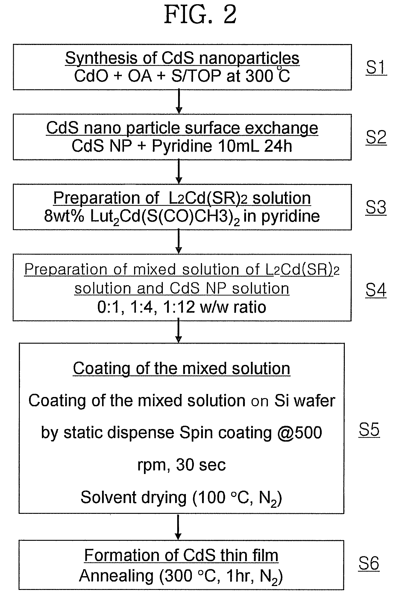
[0077]FIG. 2 illustrates the following exemplary method for preparing a thin film. In FIG. 2, step S1, 16 g of trioctylamine, 2 g of oleic acid (“OA”) and 0.4 mmol of cadmium oxide (Cdo) were simultaneously placed in a 100 ml flask equipped with a reflux condenser on a heating mantle. The reactants were stirred while maintaining constant pressure under a nitrogen atmosphere and a reaction temperature of 300° C. without any temperature gradient. The reaction temperature and stirring speed were maintained until the red cadmium oxide, turned transparent.

[0078]Separately, sulfur (S) powder was stirred in trioctylphosphine (“TOP”) under a nitrogen atmosphere to obtain a transparent solution. The concentration of the sulfur precursor solution was accordingly adjusted to about 0.25 M.

[0079]2.5 ml of the sulfur precursor solution was rapidly fed to the cadmium-containing reaction system while maintaining a temperature of 300° C., and the mixture was allowed t...

example 2

Preparation of Mixed Solution of CdS Nanoparticles and Molecular Precursor, and Preparation of Thin Film

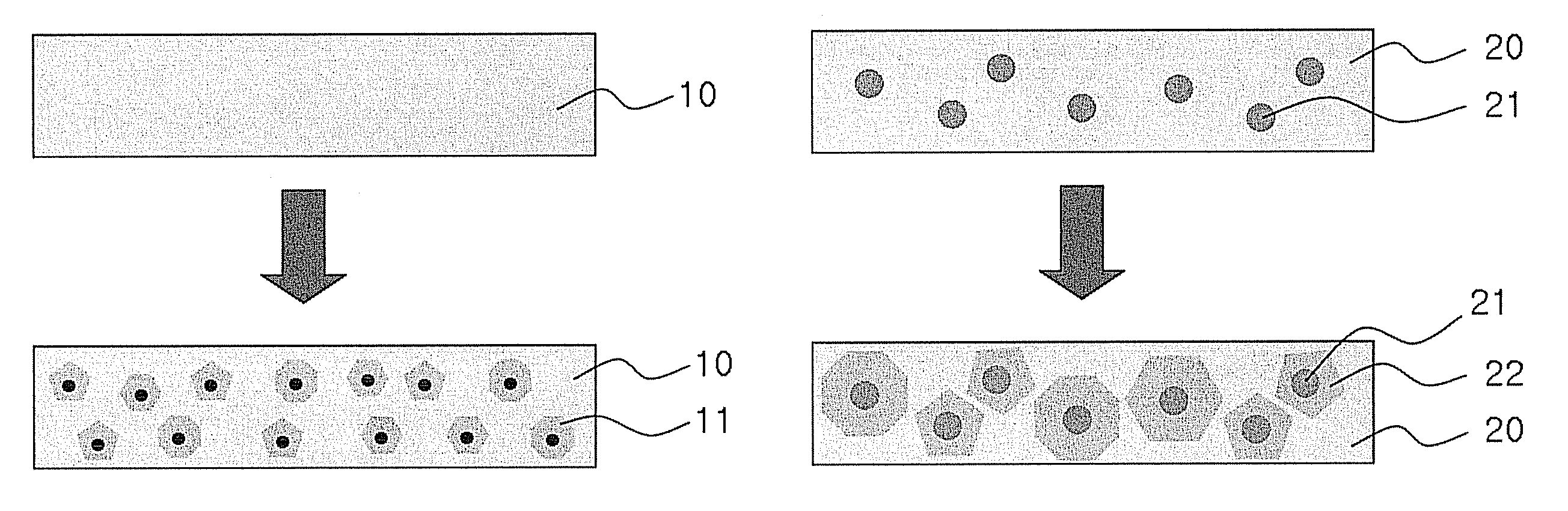
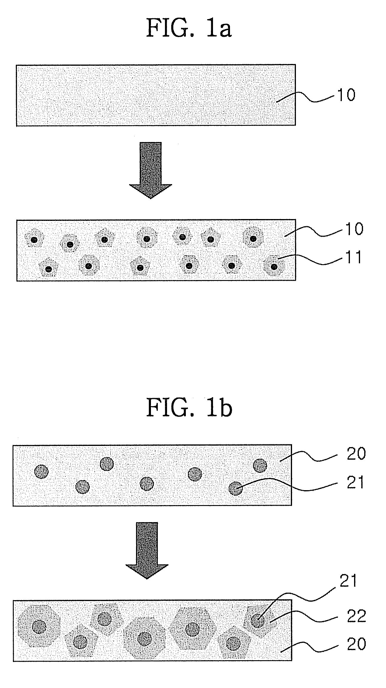
[0082]In FIG. 2, step S2, 30 mL of ethanol was added to 10 mL of the toluene dispersion of the CdS nanoparticles prepared in Example 1. The solution was centrifuged to obtain a precipitate. 10 mL of pyridine was added to the precipitate, and stirred for about 24 hours to obtain a transparent solution.

[0083]30 mL of hexane was added to the solution, followed by centrifugation. The obtained precipitate was weighed, and then pyridine was added in an amount such that the concentration of the precipitate was 2 wt %. The mixture was stirred to obtain a transparent solution.

[0084]In FIG. 2, step S3, separately, pyridine was added to a cluster of Lut2Cd(S(CO)CH3)2 to prepare a solution having a concentration of 8 wt %.

[0085]In FIG. 2, step S4, 1.5 mL of the pyridine solution of the Lut2Cd(S(CO)CH3)2 cluster (8 wt %) was mixed with 0.5 mL of the CdS nanoparticle solution to prepare a mixed...

example 3

Preparation of Mixed Solution of CdS Nanoparticles and Molecular Precursor, and Preparation of Thin Film

[0087]In FIG. 2, step S4, the procedure of Example 2 was repeated except that 1 mL of the pyridine solution of the Lut2Cd(S(CO)CH3)2 cluster (8 wt %) was mixed with 1 mL of the CdS nanoparticle solution to prepare a mixed solution of the Lut2Cd(S(CO)CH3)2 cluster (4 wt %) and the CdS nanoparticles (1 wt %). In FIG. 2, step S5, the mixed solution was coated on a Si substrate, and annealed by heating to 300° C. for one hour in FIG. 2, step S6. An X-ray diffraction pattern of the annealed substrate is shown in FIG. 5, which exhibits a crystal size of 62 Å.


PUM

PropertyMeasurementUnit
temperatureaaaaaaaaaa
wt %aaaaaaaaaa

Abstract

Disclosed herein is a thin film prepared using a mixture of nanocrystal particles and a molecular precursor. The nanocrystal is used in the thin film as a nucleus for crystal growth to minimize grain boundaries of the thin film and the molecular precursor is used to form the same crystal structure as the nanocrystal particles, thereby improving the crystallinity of the thin film. The thin film can be used effectively in a variety of electronic devices, including thin film transistors, electroluminescence devices, memory devices, and solar cells. Further disclosed is a method for preparing the thin film.

Description

[0001]This non-provisional application claims priority to Korean Patent Application No. 2006-56365, filed on Jun. 22, 2006, and all the benefits accruing therefrom under 35 U.S.C. §119(a), the content of which is herein incorporated by reference in its entirety.BACKGROUND OF THE INVENTION[0002]1. Field of the Invention[0003]The present invention relates to a thin film containing nanocrystal particles and a method for preparing the thin film. More specifically, the present invention relates to a thin film prepared using a mixture of nanocrystal particles and a molecular precursor, in which the nanocrystal is used as a nucleus for crystal growth to minimize the grain boundaries in the thin film, and the molecular precursor is used to form the same crystal structure as the nanocrystal particles, thereby improving the crystallinity of the thin film; and a method for preparing the thin film.[0004]2. Description of the Related Art[0005]Flat panel displays, such as liquid crystal displays ...

Claims


Application Information

Patent Timeline
Patent Type & Authority Patents(United States)
IPC IPC(8): C23C16/24H01L21/20
CPCC09D1/00B82Y30/00H01L21/20B82Y40/00
Inventor JANG, EUN JOOJEONG, HYUN DAMJUN, SHIN AESEON, JONG BAEK
Owner SAMSUNG ELECTRONICS CO LTD
Why Eureka
Try Eureka