

Organic electroluminescent element
a technology of electroluminescent elements and organic materials, applied in the direction of discharge tube luminescent screens, other domestic articles, natural mineral layered products, etc., can solve the problem of inability to obtain sufficient high driving durability, and achieve excellent driving durability and luminescent properties
- Summary
- Abstract
- Description
- Claims
- Application Information
AI Technical Summary
Benefits of technology
Problems solved by technology
Method used
Image

Examples
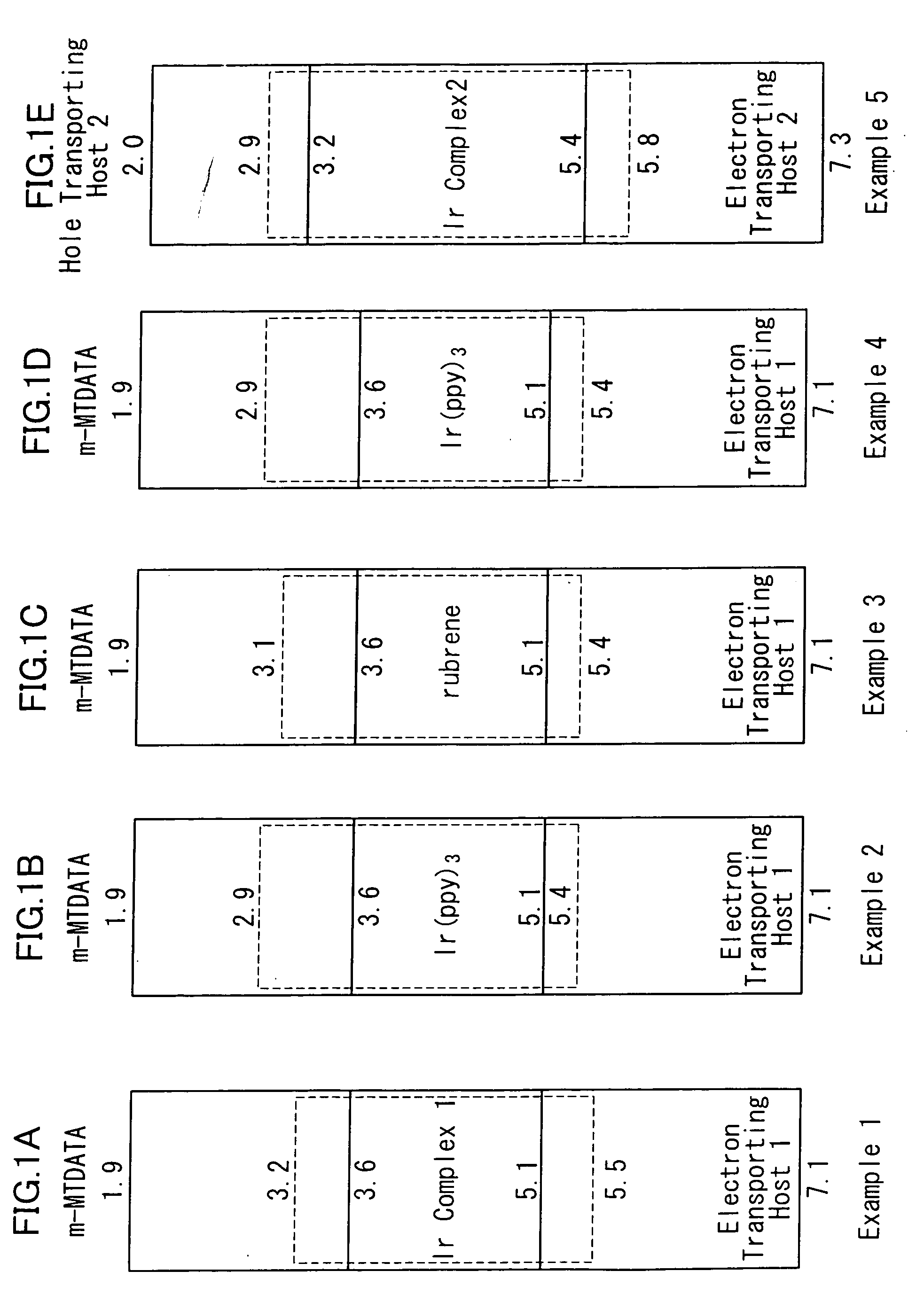
example 1
[0152] On a 2.5 cm-square glass substrate with a thickness of 0.5 mm, an ITO thin film (thickness: 0.2 μm) was formed as a transparent anode by DC magnetron sputtering (conditions: substrate temperature of 100° C., oxygen pressure of 1×10⁻³ Pa) using an ITO target having an In2O3 content of 95 mass %. The surface resistance of the ITO thin film was 10 Ω / square.
[0153] The substrate having the transparent anode formed thereon was placed in a washing vessel and subjected to IPA washing and then to UV-ozone treatment for 30 minutes. On this transparent anode, copper phthalocyanine was deposited at a rate of 0.5 nm / sec by a vacuum deposition method to provide a hole injecting layer of 10 nm.
[0154] On this hole injecting layer, 4,4′,4″-tris(2-methyl-phenylphenylamino)triphenylamine (m-MTDATA) was deposited at a rate of 0.5 nm / sec by a vacuum deposition method to provide a hole transporting layer of 40 nm.
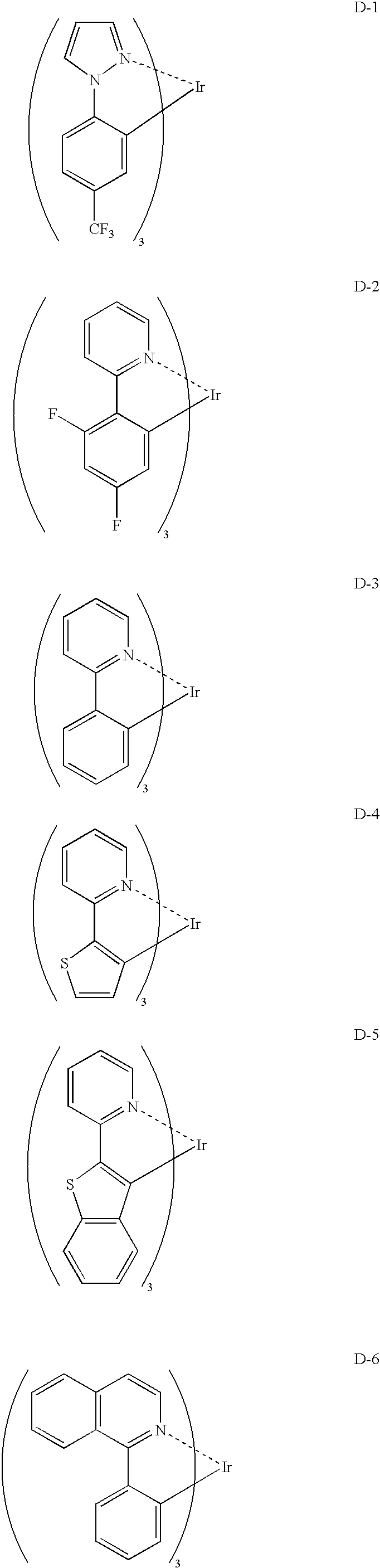
[0155] On this hole transporting layer, m-MTDATA, an electron transporting host 1 ...
example 2
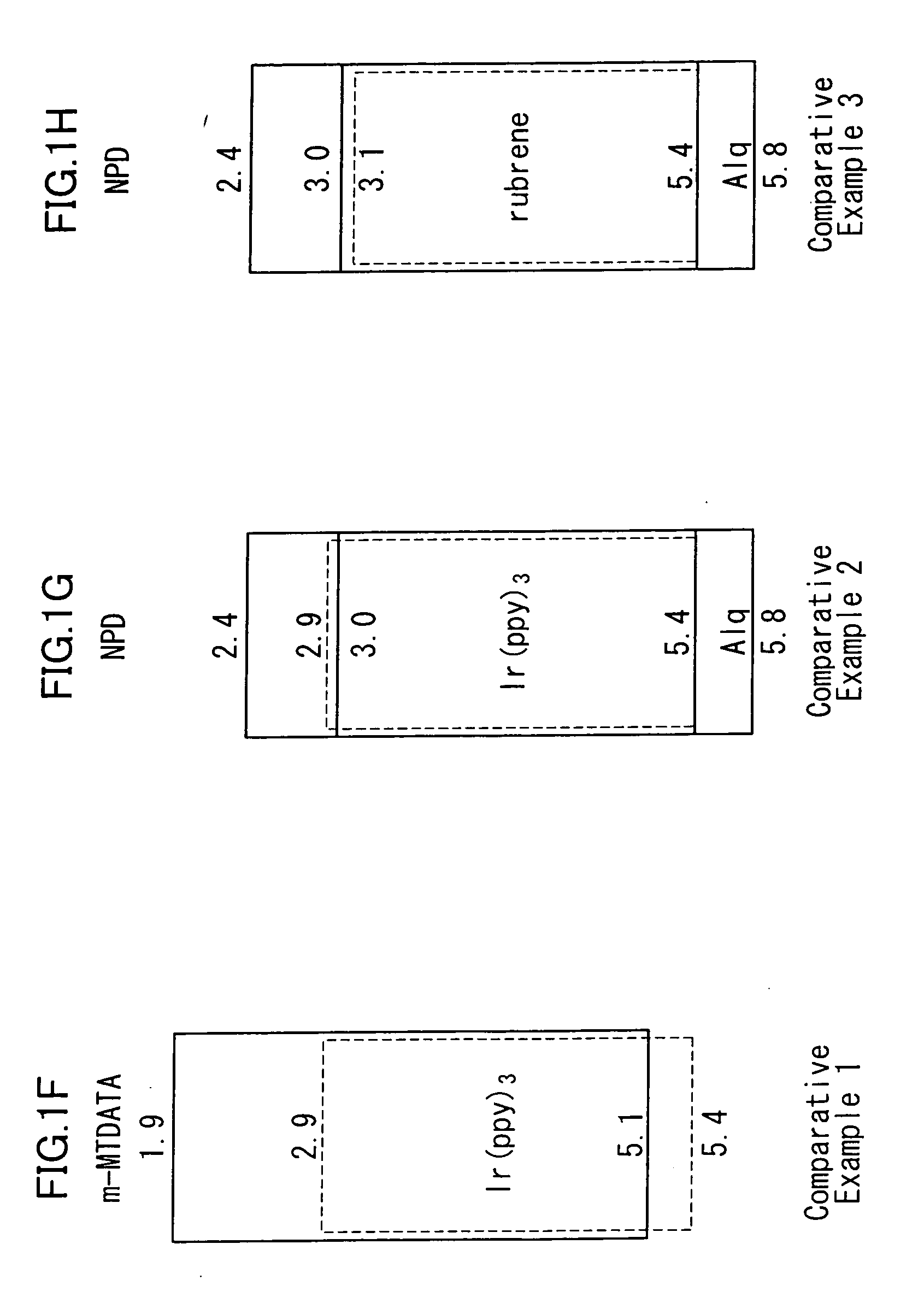
[0171] A light-emitting element was obtained in the same manner as in Example 1, except for changing Iridium Complex 1 as the luminescent dopant to Ir(ppy)3, and subjected to the same evaluation tests. The results are shown in Table 1 below.
example 3
[0172] A light-emitting element was obtained in the same manner as in Example 1, except for changing Iridium Complex 1 as the luminescent dopant to rubrene, and subjected to the same evaluation tests. The results are shown in Table 1 below.
PUM
| Property | Measurement | Unit |
|---|---|---|
| thickness | aaaaa | aaaaa |
| thickness | aaaaa | aaaaa |
| thickness | aaaaa | aaaaa |
Abstract
Description
Claims
Application Information