Semiconductor integrated circuit device
- Summary
- Abstract
- Description
- Claims
- Application Information
AI Technical Summary
Benefits of technology
Problems solved by technology
Method used
Image

Examples
first embodiment
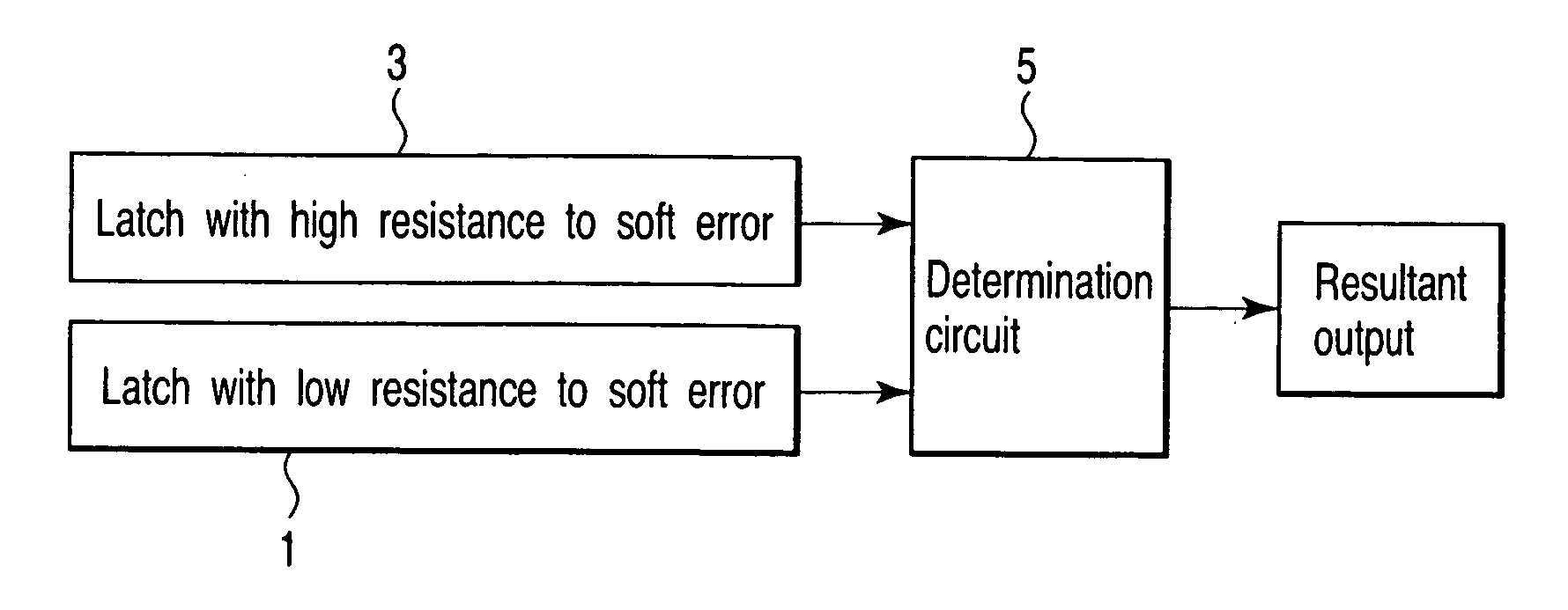
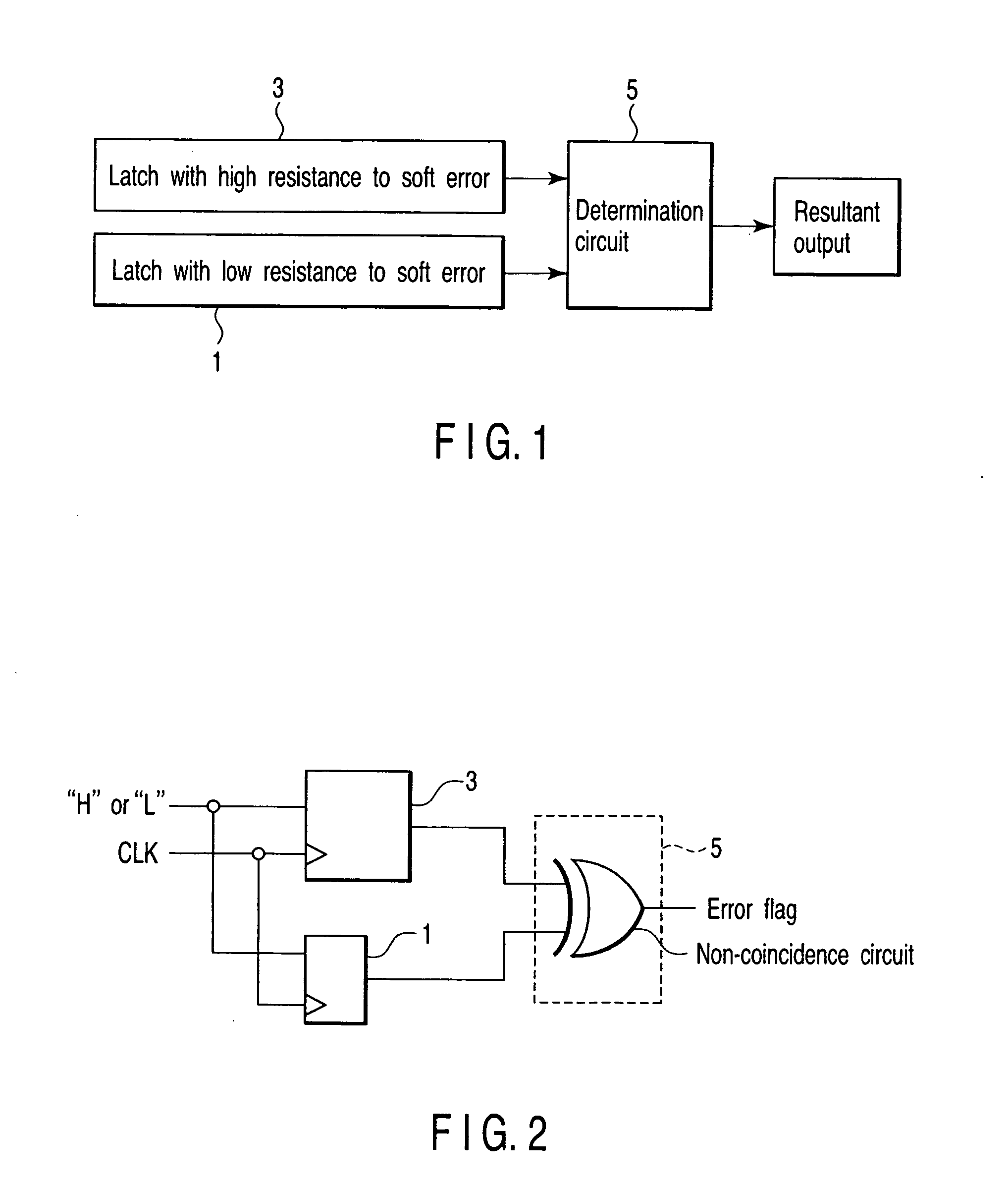
[0030]FIG. 1 is a block diagram showing an example of the basic configuration of a semiconductor integrated circuit device according to a first embodiment of this invention.
[0031] As shown in FIG. 1, the integrated circuit device according to the first embodiment includes latch circuits 1, 3. The latch circuit 1 has low resistance to soft errors and the latch circuit 3 has higher resistance to soft errors in comparison with the latch circuit 1. In the following explanation, the terms “low-resistance latch circuit 1” and “high-resistance latch circuit 3” are used.
[0032] For example, a determination circuit 5 compares data read out from the low-resistance latch circuit 1 with data read out from the high-resistance latch circuit 3 to determine whether the data is true or not. That is, the determination circuit 5 determines whether data held in the low-resistance latch circuit 1 is true or not based on data held in the high-resistance latch circuit 3.
[0033]FIG. 2 is a circuit diagram...
first circuit example
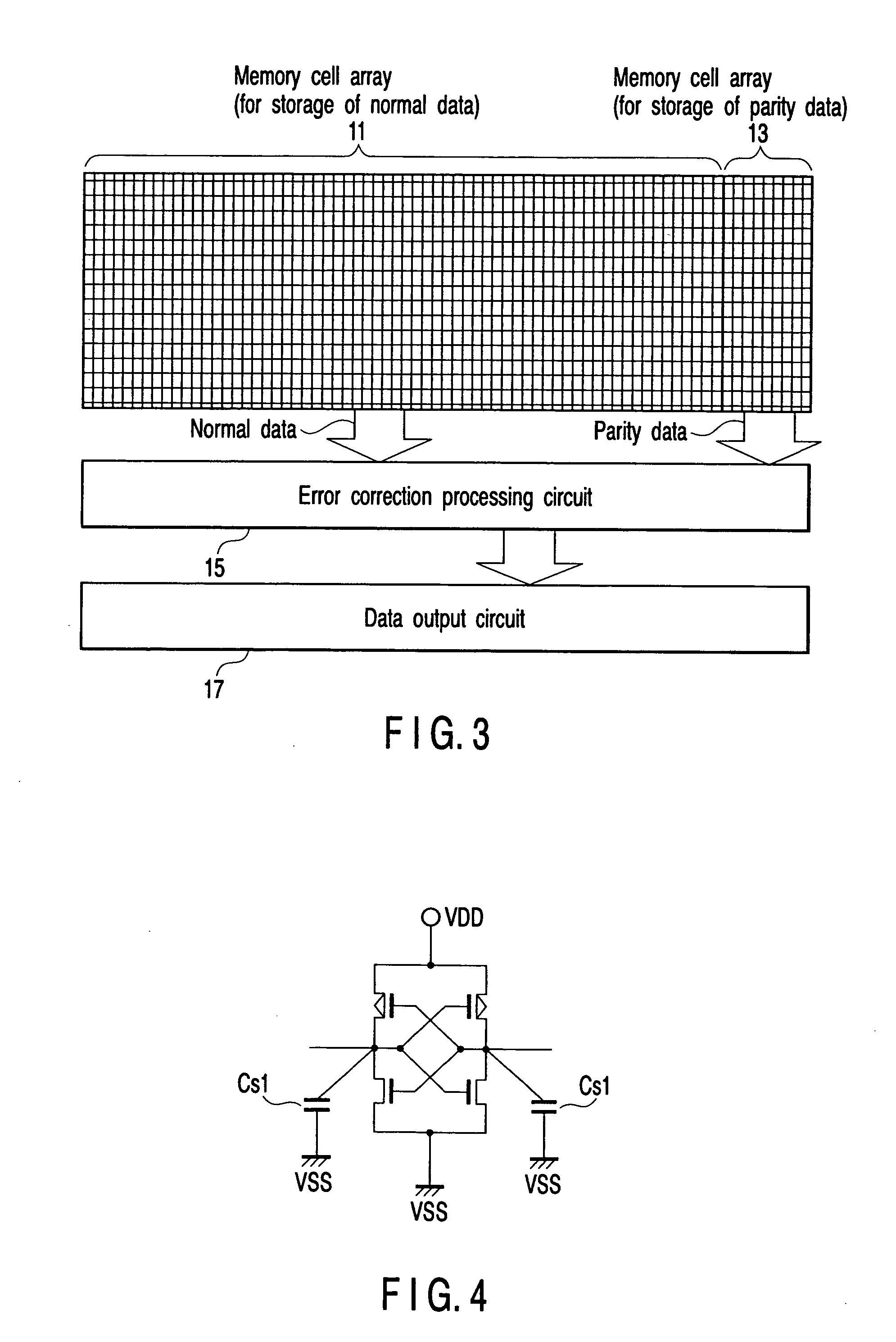
[0044]FIG. 4 is a circuit diagram showing a first circuit example of the low-resistance latch circuit and FIG. 5 is a circuit diagram showing a first circuit example of the high-resistance latch circuit.
[0045] As shown in FIGS. 4 and 5, the difference between the low-resistance latch circuit and high-resistance latch circuit lies in the capacitance of the storage node. In this example, the capacitance of the storage node of the low-resistance latch circuit is “Cs1”. On the other hand, the capacitance of the storage node of the high-resistance latch circuit is “Cs2” and, in this case, “Cs2>Cs1”. In order to form a high-resistance latch circuit, it is only necessary to attach capacitance larger than the capacitance of the low-resistance latch circuit to the storage node of the circuit. One example of the capacitance can be attained by a capacitor, for example. The low-resistance latch circuit and high-resistance latch circuit can be attained in one integrated circuit chip by attachin...
second circuit example
[0047]FIG. 6 is a circuit diagram showing a second circuit example of the high-resistance latch circuit.
[0048] As shown in FIG. 6, in the high-resistance latch circuit of the second circuit example, the size of a transistor configuring the high-resistance latch circuit is made larger than the size of a transistor configuring the low-resistance latch circuit. As the size of the transistor becomes larger, the capacitance “Cs2” of the storage node increases to form a high-resistance latch circuit. An example in which the size of the transistor is changed is explained below.
[0049]FIG. 7A is a plan view showing a transistor with low-level driving ability and FIG. 7B is a plan view showing a transistor with high-level driving ability.
[0050] As shown in FIGS. 7A, 7B, in the example in which the size of the transistor is changed, various degrees of the driving ability are provided. The driving ability of the transistor, particularly, the current driving ability depends on the gate width ...
PUM
 Abstract
Description
Claims
Application Information
 - R&D Engineer
- R&D Manager
- IP Professional
- Industry Leading Data Capabilities
- Powerful AI technology
- Patent DNA Extraction
Browse by: Latest US Patents, China's latest patents, Technical Efficacy Thesaurus, Application Domain, Technology Topic.
© 2024 PatSnap. All rights reserved.Legal|Privacy policy|Modern Slavery Act Transparency Statement|Sitemap