Interconnect layout method

a layout method and interconnect technology, applied in the field of interconnect layout methods, can solve the problems of reducing limiting the effect of forming gates, and ignoring shape fluctuations, so as to improve the yield of semiconductor devices, reduce imaging fluctuations, and reduce the shape of gate patterns which occur by repetition of exposure shots

Inactive Publication Date: 2006-04-20
RENESAS ELECTRONICS CORP
View PDF7 Cites 228 Cited by
  • Summary
  • Abstract
  • Description
  • Claims
  • Application Information

AI Technical Summary

Benefits of technology

[0013] According to the present invention, the gate patterns and the dummy patterns are arranged so that the first predetermined distance, the second predetermined distance, and the third predetermined distance are the numeric value that is within the range from −10% to +10% of the exposure wavelength λ while centering around the numeric value that is a natural number multiple of the wavelength of the light (“exposure light”) used for exposure of the gate patterns. A diffracted light of the exposure light is, therefore, reduced and the fluctuations of imaging are reduced. Thus, fluctuations in the shape of the gate patterns which occur by repetition of the exposure shots may be reduced. As a result of this, the semiconductor device yield may be improved.
[0014] According to the present invention, the first predetermined distance, the second predetermined distance, and the third predetermined distance are the numeric value that falls within the range from −10% to +10% of the exposure wavelength λ and that centers around the numeric value that is a natural number multiple of the wavelength of the light used for exposure of the gate patterns. It is, therefore, possible to reduce the fluctuations in shape of the gate patterns and improve the semiconductor device yield.

Problems solved by technology

However, this effect is limited to a step for forming gates and no consideration is given to fluctuations in shape of the gate patterns that repeatedly occur by repetition of optical shot into a silicon wafer.
In addition, even if patterns are equal in shape, the semiconductor device yield is not improved yet in the conventional gate layout method for repeatedly performing exposure shots into the silicon wafer a number of times.

Method used


Image

  • Interconnect layout method
  • Interconnect layout method
  • Interconnect layout method

Examples


Embodiment Construction

[0021] The invention will be now described herein with reference to illustrative embodiments. Those skilled in the art will recognize that many alternative embodiments can be accomplished using the teachings of the present invention and that the invention is not limited to the embodiments illustrated for explanatory purposed.

[0022] An exemplary embodiment of the present invention will be described hereinafter with reference to the drawings. Like constituent elements are denoted by the same reference symbols throughout the drawings, and they will not be repeatedly described.

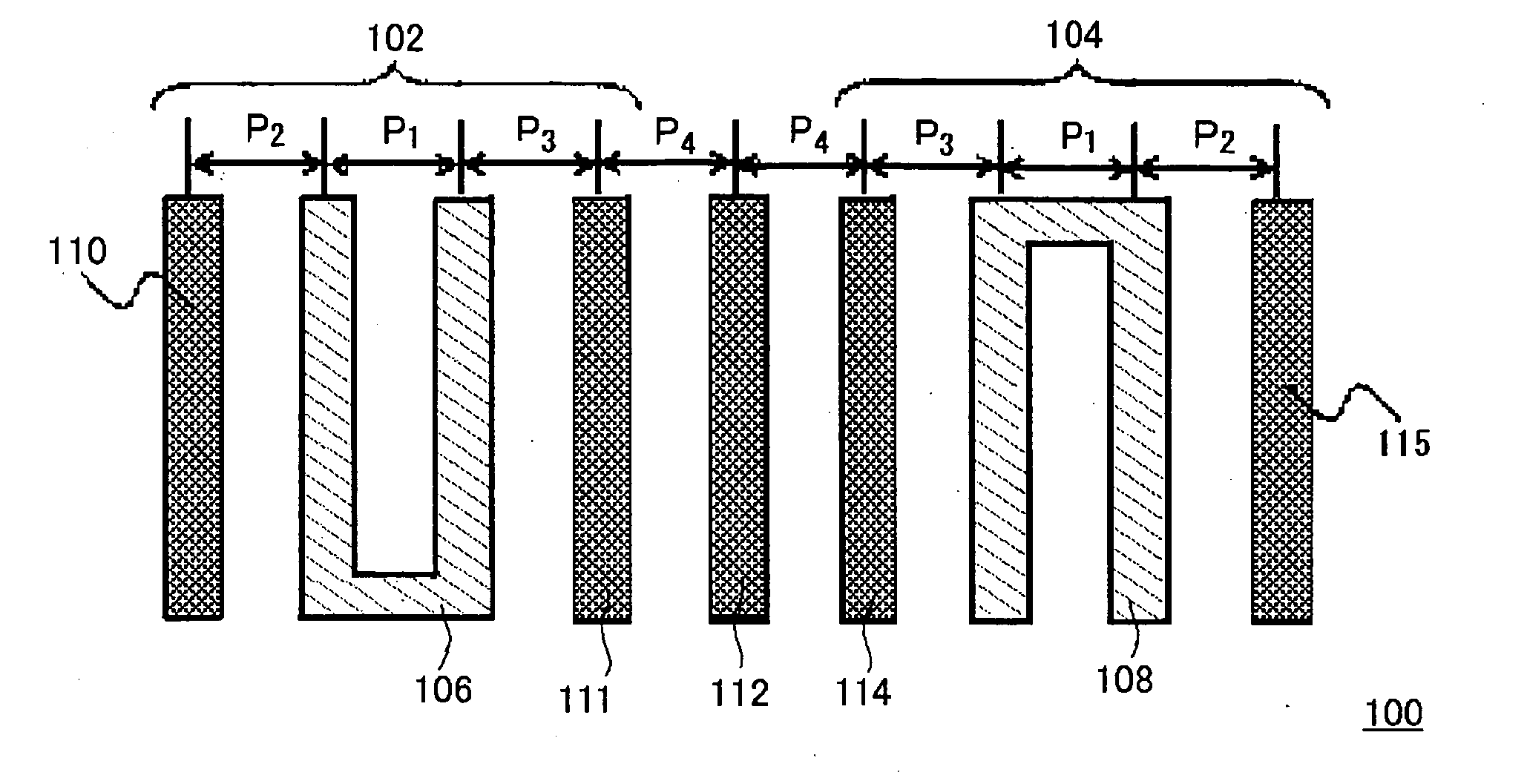
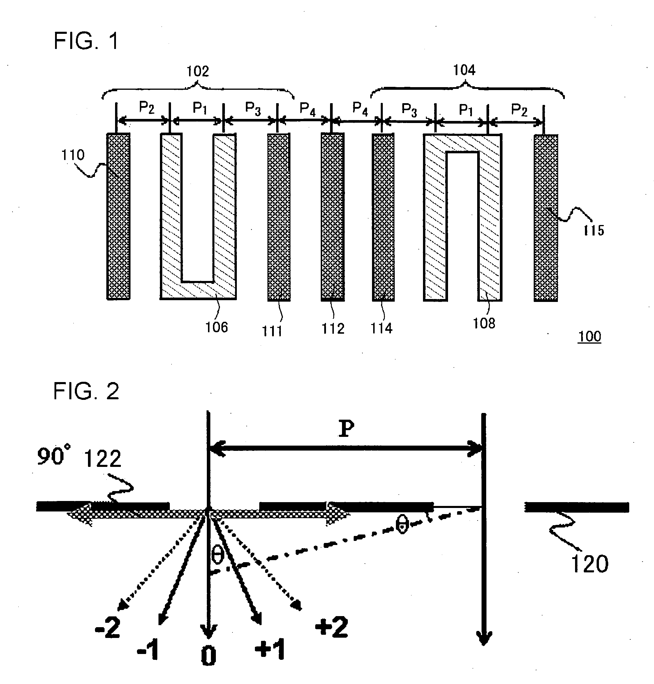
[0023] In an interconnect layout 100 shown in FIG. 1, a first gate pattern and a second gate pattern provided substantially in parallel to each other at a first predetermined distance therebetween, a first dummy pattern (dummy interconnect 110) that is provided to be adjacent to the first gate pattern on an opposite side to a side on which the second gate pattern is provided at a second predetermined distance fr...


PUM

PropertyMeasurementUnit
wavelengthaaaaaaaaaa
distanceaaaaaaaaaa
center-to-center distance P4aaaaaaaaaa

Abstract

An interconnect layout method capable of reducing variations in shape of gate patterns and improving yield of a semiconductor device is provided. In an interconnect layout 100, the first gate pattern, the second gate pattern, the first dummy pattern, and the second dummy pattern are arranged so that, if a wavelength of a light used to expose the first gate pattern and the second gate pattern is λ, natural numbers are m1, m2, and m3, the first predetermined distance is P1, the second predetermined distance is P2, the third predetermined distance is P3, a design value of the first predetermined distance is P1′, a design value of the second predetermined distance is P2′, and a design value of the third predetermined distance is P3′, then the first predetermined distance satisfies relationships of P1=m1λ and P1′−0.1λ≦P1≦P1′+0.1λ, the second predetermined distance satisfies relationships of P2=m2λ and P2′−0.1λ≦P2≦P2′+0.1λ, and the third predetermined distance satisfies relationships of P3=m3λ and P3′−0.1λ≦P3≦P3′+0.1λ.

Description

[0001] This application is based on Japanese Patent application NO. 2004-304309, the content of which is incorporated hereinto by reference. BACKGROUND OF THE INVENTION [0002] 1. Field of the Invention [0003] The present invention relates to an interconnect layout method. [0004] 2. Related Art [0005] Recently, following high integration and reduction in size of semiconductor devices, fluctuations in shape of gate patterns during forming the gate patterns has greatly influenced on fluctuations in electric characteristics such as an ON current and a threshold voltage. It is, therefore, required to provide a technique for controlling fluctuations in shape of the gate patterns so as to improve semiconductor device yield by improving the electric characteristics. [0006] As shown in FIG. 4, in a conventional gate layout as disclosed in Japanese Laid-open patent publication No. 1997-311432 (No. H09-311432), a so-called vacant area 9 is present between actual patterns 8a to 8d and actual pa...

Claims


Application Information

Patent Timeline
Patent Type & Authority Applications(United States)
IPC IPC(8): H01L21/4763H01L21/3205G03F1/68G03F1/70H01L21/027H01L21/82H01L21/822H01L27/04
CPCH01L23/522H01L27/0207H01L2924/0002H01L2924/00
Inventor IWAKI, TAKAYUKI
Owner RENESAS ELECTRONICS CORP
Why Eureka
Try Eureka