Organic thin-film transistor, method of fabricating the same, and flat panel display having the same

a thin-film transistor and flat-panel display technology, applied in the direction of basic electric elements, electrical appliances, semiconductor devices, etc., can solve the problems of undesired leakage current and very vulnerable plastic substrate to hea

Active Publication Date: 2006-05-11
SAMSUNG DISPLAY CO LTD
View PDF9 Cites 11 Cited by
  • Summary
  • Abstract
  • Description
  • Claims
  • Application Information

AI Technical Summary

Benefits of technology

[0013] The present invention provides an organic thin film transistor (OTFT), a method of fabricating the same, and an organic electroluminescent d

Problems solved by technology

As the plastic substrate is very vulnerable to heat, the flexible organic electroluminescent display device must be fabricated using a low temperature process.
Howev

Method used


Image

  • Organic thin-film transistor, method of fabricating the same, and flat panel display having the same
  • Organic thin-film transistor, method of fabricating the same, and flat panel display having the same
  • Organic thin-film transistor, method of fabricating the same, and flat panel display having the same

Examples


Embodiment Construction

[0029] The present invention will be described more fully hereinafter with reference to the accompanying drawings, in which preferred embodiments of the invention are shown. This invention may, however, be embodied in many different forms and should not be construed as being limited to the embodiments set forth herein. Rather, these embodiments are provided so that this disclosure will be thorough and complete, and will fully convey the scope of the invention to those skilled in the art. In the drawings, the thicknesses of layers and regions are exaggerated for clarity. Like numbers refer to like elements throughout the specification.

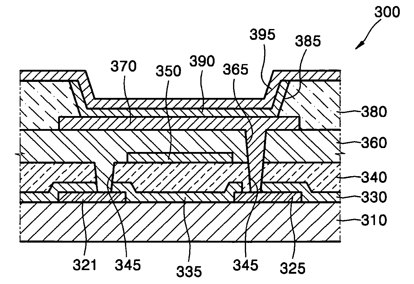
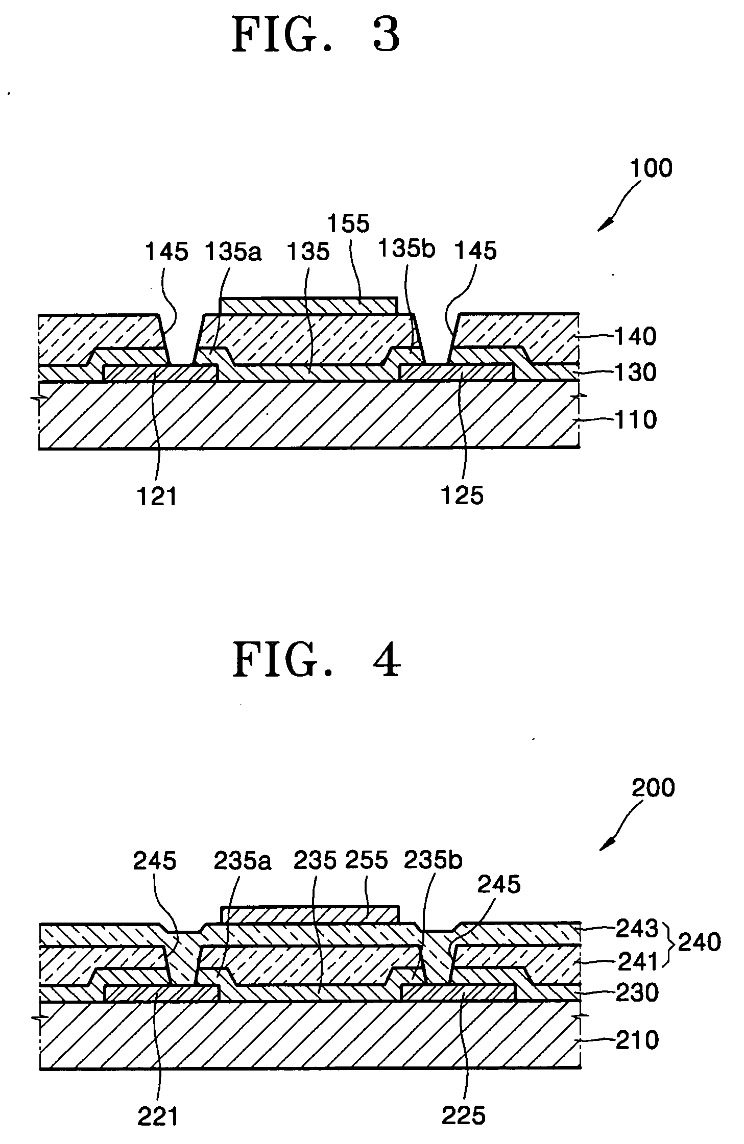
[0030]FIG. 3 is a sectional view that illustrates an organic thin-film transistor (OTFT) used in a flexible organic electroluminescent display device according to an embodiment of the present invention.

[0031] Referring to FIG. 3, an OTFT 100 according to an embodiment of the present invention includes a source electrode 121 and a drain electrode 125 f...


PUM


Abstract

The present invention relates to an organic thin film transistor (OTFT), a method of fabricating the OTFT, and an organic electroluminescent display that has the OTFTs. The invention prevents surface damage of an organic semiconductor layer and reduces an off-current. The OTFT includes a substrate, a source electrode and a drain electrode formed on the substrate, and a semiconductor layer formed on the substrate that has a channel layer disposed over and between the source electrode and drain electrode. In addition, the OTFT includes a gate insulating layer formed on the semiconductor layer, a separation pattern formed through the semiconductor layer and the gate insulating layer to separate the channel layer, and a gate electrode formed on the gate insulating layer over the channel layer.

Description

BACKGROUND OF THE INVENTION [0001] This application claims the priority to and benefit of Korean Patent Application No. 10-2004-0091522, filed on Nov. 10, 2004, in the Korean Intellectual Property Office, the disclosure of which is incorporated herein in its entirety by reference. [0002] 1. Field of the Invention [0003] The present invention relates to a thin-film transistor (TFT) for a flat panel display. More particularly, the present invention relates to an organic thin-film transistor (OTFT) for preventing damages on the surface of an organic semiconductor layer, a method of fabricating the same, and a flat panel display having the same. [0004] 2. Description of the Related Art [0005] An organic thin-film transistor (OTFT) is a drive element for a next generation display that has been actively studied. The OTFT uses an organic material instead of silicon as a semiconductor layer. Depending on the compositional material of the organic layer, there are a low molecular weight OTFTs...

Claims


Application Information

Patent Timeline
IPC IPC(8): H01L31/0376
CPCH01L27/3244H01L51/0541H10K59/12H10K10/464
Inventor AHN, TAEKKOO, JAE-BONSUH, MIN-CHUL
Owner SAMSUNG DISPLAY CO LTD
Why Eureka
Try Eureka