Flat panel display and its method of fabrication

a technology of display device and flat panel, which is applied in the direction of electroluminescent light source, organic semiconductor device, electric lighting source, etc., can solve the problems of non-uniform power supply voltage supplied to a pixel according to the arrangement position of the pixel, image quality degradation, non-uniform brightness, etc., and achieve the effect of preventing line defects

Inactive Publication Date: 2006-05-18
SAMSUNG DISPLAY CO LTD
View PDF19 Cites 23 Cited by
  • Summary
  • Abstract
  • Description
  • Claims
  • Application Information

AI Technical Summary

Benefits of technology

[0015] The present invention provides a flat panel display device which can prevent line defects and voltage drops using a substrate formed of metal foil as a power supply layer and its method of fabrication.

Problems solved by technology

Thus, when a power supply voltage is supplied to a pixel via the power supply line, due to voltage drop caused by the power supply line formed in a line shape, the power supply voltage supplied to a pixel according to the arrangement position of the pixel becomes non-uniform.
As a result, non-uniform brightness occurs and image quality is degraded.
In addition, when two adjacent signal lines are arranged on one layer, due to extraneous particles formed during fabrication, a short between the data line and the power supply line can occur.

Method used


Image

  • Flat panel display and its method of fabrication
  • Flat panel display and its method of fabrication
  • Flat panel display and its method of fabrication

Examples


Embodiment Construction

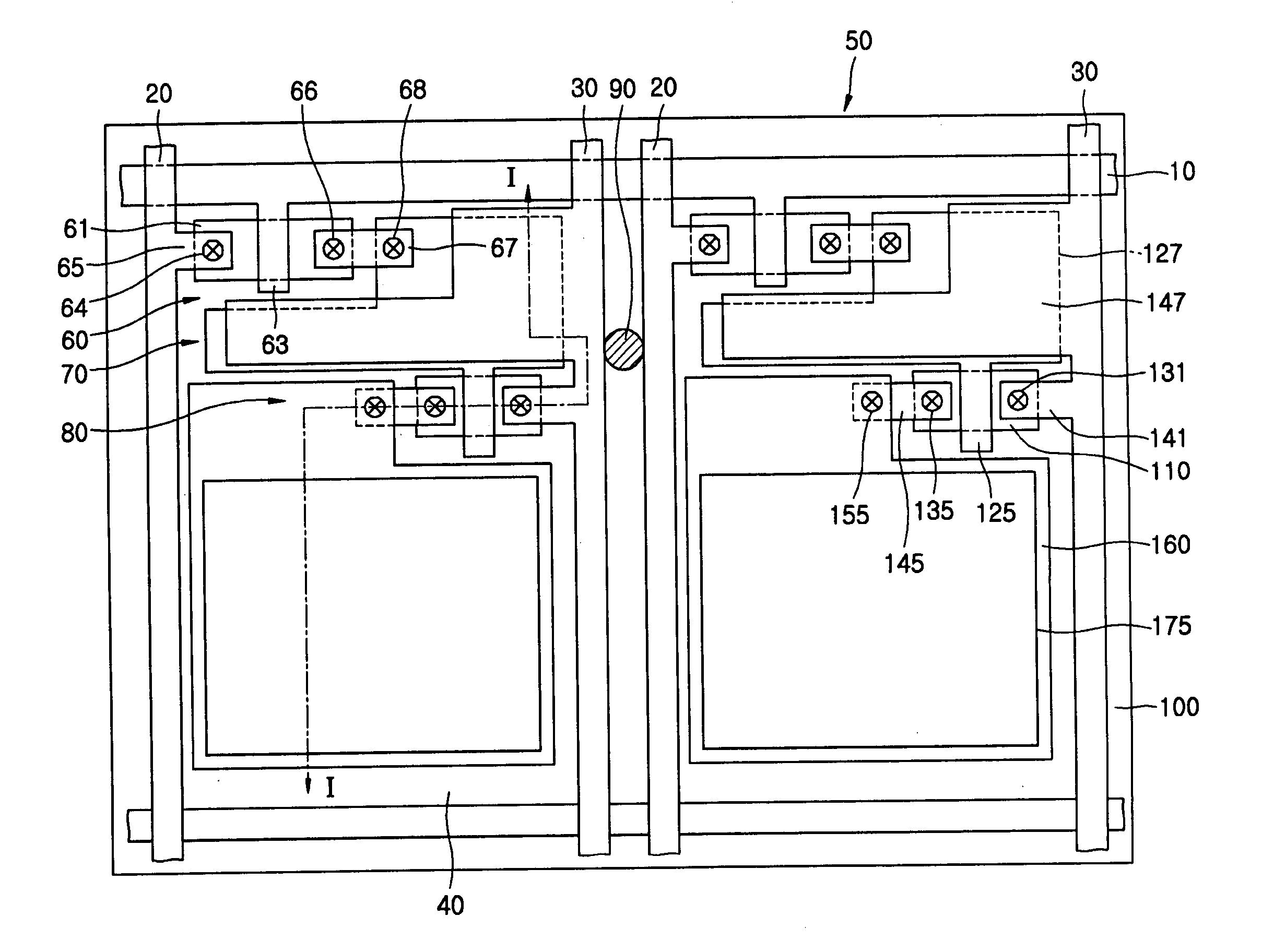
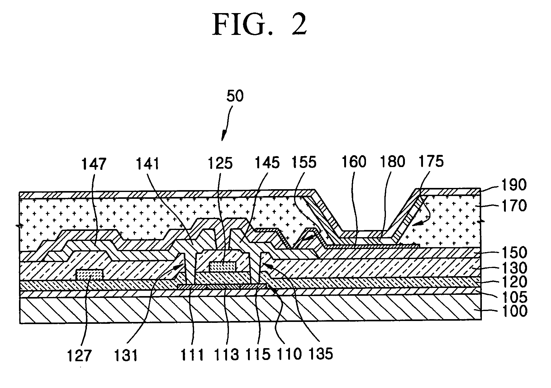
[0043]FIG. 1 is a plan view of an OELD apparatus. The OELD of FIG. 1 includes a gate line 10, a data line 20, a power supply line 30, and a pixel 50 arranged in a pixel region 40. The pixel 50 includes a switching Thin Film Transistor (TFT) 60, a capacitor 70, a driving Thin Film Transistor (TFT) 80, and an organic Electro-Luminescent (EL) element having a pixel electrode 160.

[0044] The switching TFT 60 includes a semiconductor layer 61, a gate electrode 63, and source and drain electrodes 65 and 67 each being respectively connected to the semiconductor layer 61 via contact holes 64 and 66. The capacitor 70 includes a lower electrode 127 and an upper electrode 147, which are connected to the drain electrode 67 of the switching TFT 60 via a contact hole 68.

[0045] The driving TFT 80 includes a semiconductor layer 110, a gate electrode 125, and a source electrode 141 and a drain electrode 145 each being respectively connected to the semiconductor layer 110 via contact holes 131 and 1...


PUM


Abstract

A flat panel display device which can prevent line defects and voltage drops using a conductive substrate formed of metal foil as a power supply layer includes: a conductive substrate; a first insulating layer formed on one side of the substrate and having a contact hole exposing a part of the conductive substrate; a Thin Film Transistor (TFT) having a semiconductor layer formed on the first insulating layer, a gate electrode, and source and drain electrodes; and a display element having a pixel electrode connected to one of the source and drain electrodes of the TFT. The other of the source and drain electrodes of the TFT is electrically connected to the conductive substrate via the contact hole.

Description

CLAIM OF PRIORITY [0001] This application makes reference to, incorporates the same herein, and claims all benefits accruing under 35 U.S.C. §119 from an application for ORGANIC LIGHT EMITTING DEVICE AND METHOD FOR FABRICATING THE SAME earlier filled in the Korean Intellectual Property Office on 18 Nov. 2004 and there duly assigned Serial No. 10-2004-0094512. BACKGROUND OF THE INVENTION [0002] 1. Field of the Invention [0003] The present invention relates to a flat panel display device, and more particularly, to a flexible Organic Electro-Luminescent Display (OELD) using a metal foil substrate as a power supply layer and its method of fabrication. [0004] 2. Description of the Related Art [0005] Organic Electro-Luminescent Display (OELD) elements are self-emission display elements in which light is emitted from an emission layer according to voltages supplied to two electrodes between which the emission layer is interposed. OELD elements have advantages such as wider view-angle than ...

Claims


Application Information

Patent Timeline
Patent Type & Authority Applications(United States)
IPC IPC(8): H01L29/04
CPCH01L27/3276H01L51/52H01L2251/5338H01L51/0096H10K59/131H10K77/10H10K50/80H10K2102/311H05B33/26H05B33/10
Inventor SHIN, HYUN-SOOKOO, JAE-BONMO, YEON-GON
Owner SAMSUNG DISPLAY CO LTD
Why Eureka
Try Eureka