Plasma display panel

a technology of display panel and plasma, which is applied in the manufacture of electric discharge tube/lamp, discharge tube luminescence screen, electrode system, etc., can solve the problems of increased discharge firing voltage, increased manufacturing cost of pdp, and loss of input energy applied to cathodes and anodes due to inefficiencies, etc., to achieve enhanced luminescence efficiency and reduce discharge firing voltage

Inactive Publication Date: 2006-05-18
SAMSUNG SDI CO LTD
View PDF27 Cites 8 Cited by
  • Summary
  • Abstract
  • Description
  • Claims
  • Application Information

AI Technical Summary

Benefits of technology

[0018] One embodiment of the present invention provides a PDP with an opposing electrode structure which has reduced discharge firing voltage and enhanced luminescence efficiency.

Problems solved by technology

While passing through the above steps, input energy applied to a cathode and an anode is lost due to inefficiencies.
However, increase in the positive column region or increase in the partial pressure of Xe, result in an increased discharge firing voltage, which causes the manufacturing cost of the PDP to be increased.

Method used


Image

  • Plasma display panel
  • Plasma display panel
  • Plasma display panel

Examples


first embodiment

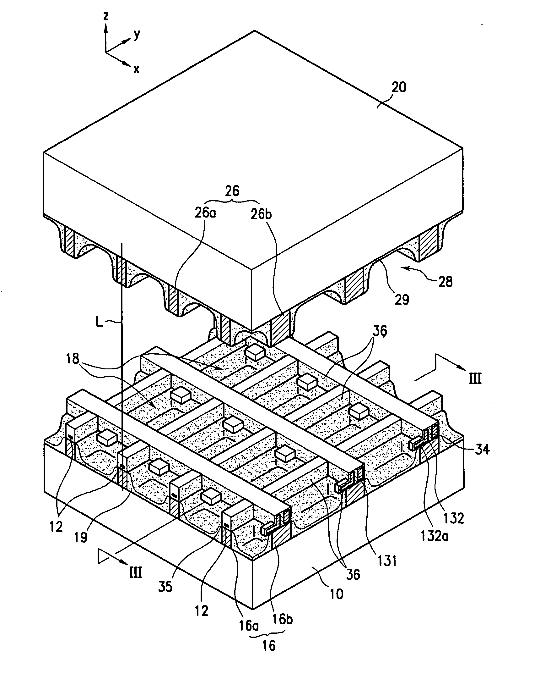
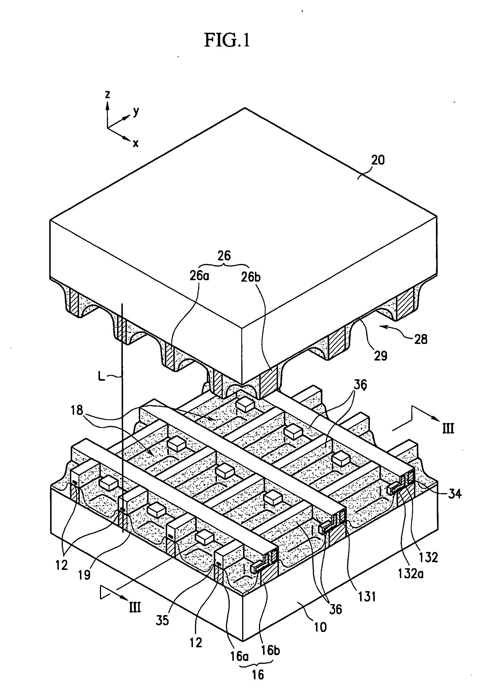
[0115] Further, in order to induce the opposing electrode discharge over a wider area, the sustain electrodes 131 and the scan electrodes 132 have expansion portions 131b, 132b in the discharge cells 17. The expansion portions 131b, 132b are shown in FIG. 4 that is a perspective view of the electrodes in the PDP of the present invention. The expansion portions 131b, 132b extend in the z-axis direction of FIG. 4 which is a direction perpendicular to the rear substrate 10.

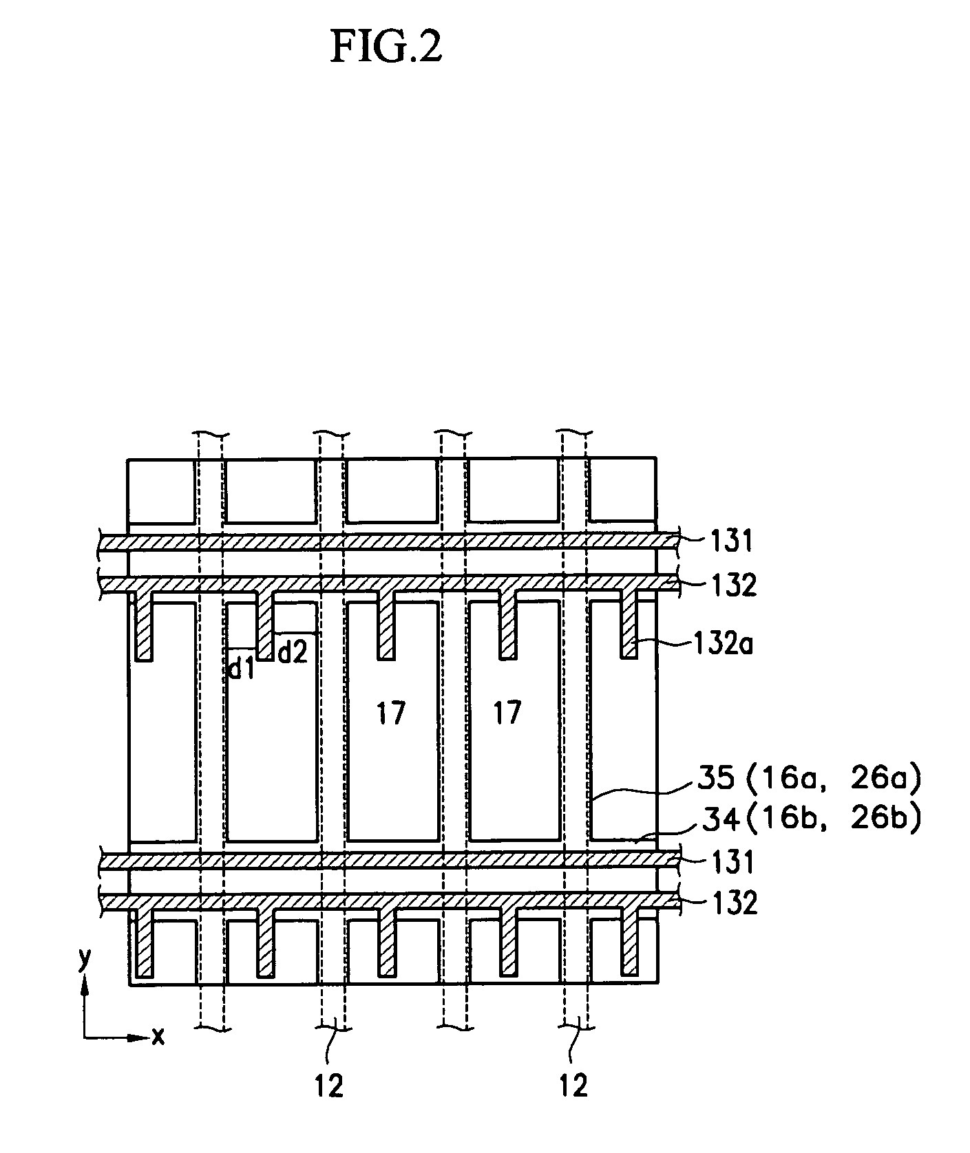
[0116] Referring to the x-z cross-section of the expansion portions 131b, 132b, shown in FIG. 3, indicates that a length hv in the vertical direction is longer than a length hh in the horizontal direction.

[0117] The opposing electrode discharge is generated over a larger area by using the expansion portions 131b, 132b and therefore generates more intense vacuum ultraviolet rays. The intense vacuum ultraviolet rays generated, collide against the first and second phosphor layers 19, 29 inside the discharge cells 17, i...

second embodiment

[0138]FIG. 6 is a plan view of electrodes and discharge cells in a PDP according to the present invention. Sustain electrodes 231 and scan electrodes 232 are located in parallel pairs along a direction (x-axis direction) crossing the direction of the address electrodes 12 (y-axis direction). In two adjacent discharge cells 17, located along the direction of the address electrodes 12 (along the y-axis direction), the sustain and scan electrodes 231, 232 alternate but the scan electrodes 232 of the two adjacent discharge cells 28, 28 are also adjacent. In other words, the sustain and scan electrodes 231, 232 are located in the following order: the sustain electrode 231, the scan electrode 232, another scan electrode 232, and then the sustain electrode 231, followed by another pair of adjacent scan electrodes 232, 232.

[0139] In this embodiment, between the third and fourth barrier rib members 16b, 26b of one side of the discharge cell 17, two scan electrodes 232 for two adjacent discha...

fourth embodiment

[0142] In the fourth embodiment, a protrusion 432c is further provided in a protruding portion 432a of a scan electrode 432. The protruding portion 432a of the scan electrode 432 is closer to the address electrode 12 on one side of the discharge cell 17, and thus the protrusion 432c formed on the protruding portion 432a is even closer to this address electrode 12.

[0143] The protruding portion 432a is formed to protrude from the expansion portion 432b toward the center of the discharge cell 17 and the protrusion 432c is formed to protrude from the protruding portion 432a toward one of the address electrodes 12 on one side of the discharge cells 17.

[0144] Therefore, the protruding portion 432a of the scan electrode 432 and its protrusion 432c form a shorter gap with the address electrode 12 of one side of the discharge cell 17, and the address discharge can be generated with a low voltage. The protrusion 432c facing the address electrode 12 of one side is formed in the protruding por...


PUM


Abstract

A PDP having an opposing electrode structure including first and second substrates facing each other. A space between the first and second substrates is divided into discharge cells. Address electrodes extend in a first direction between the first and second substrates, and first and second electrodes extend in a second direction intersecting the first direction while being spaced apart from the address electrodes. At least one of the address electrodes or the first and second electrodes has a protruding portion that protrudes toward the center of each discharge cell. The protruding portions help reduce the discharge gap which in turn reduces the discharge firing voltage. Expansion portions formed as parts of the first and second electrodes increase the discharge gap used by the sustain discharge and lead to an improved luminescence efficiency.

Description

CROSS REFERENCES TO RELATED APPLICATIONS [0001] This application claims priority to and the benefit of Korean Patent Applications No. 10-2004-0093919 and No. 10-2004-0093920 filed in the Korean Intellectual Property Office both on the same day of Nov. 17, 2004, the entire contents of which are incorporated herein by reference. FIELD OF THE INVENTION [0002] The present invention relates to a plasma display panel, and more particularly, to a plasma display panel that can reduce a discharge firing voltage and improve luminescence efficiency. BACKGROUND OF THE INVENTION [0003] Generally, a plasma display panel (PDP) has a three-electrode surface-discharge structure. The PDP having the three-electrode surface-discharge structure includes front and rear substrates. A discharge gas is sealed between the two substrates. [0004] The front substrate has sustain electrodes and scan electrodes that extend in one direction on the inner surface of the front substrate. The rear substrate is spaced ...

Claims


Application Information

Patent Timeline
Patent Type & Authority Applications(United States)
IPC IPC(8): H01J61/00H01J11/14H01J11/16H01J11/22H01J11/24H01J11/26H01J11/32H01J11/34H01J11/36H01J11/38H01J11/42
CPCH01J11/16H01J11/24H01J2211/245
Inventor HUR, MINCHOI, HOON-YOUNGCHOI, YOUNG-DOMIZUTA, TAKAHISA
Owner SAMSUNG SDI CO LTD
Why Eureka
Try Eureka