Passivation film and method of forming the same

a technology of passivation film and film layer, which is applied in the manufacture of electrode systems, superimposed coating processes, electric discharge tubes/lamps, etc., can solve the problems of discharge firing voltage and power consumption, reduce the potential barrier of secondary electron emission, and generate defects at the interface between mgo layer and intervening layer, so as to reduce the total power consumption of pdp. , the effect of preventing deformation of pdp and preventing the characteristi

Inactive Publication Date: 2009-04-02
LG ELECTRONICS INC
View PDF1 Cites 1 Cited by
  • Summary
  • Abstract
  • Description
  • Claims
  • Application Information

AI Technical Summary

Benefits of technology

[0021]In accordance with the exemplary embodiments, the first MgO layer, the intervening layer, and the second MgO layer are laminated and the laser is then irradiated to oxidize the intervening layer. Simultaneously, defects are generated at the interface between the first and second MgO layers, and the intervening layer. Therefore, the plasma discharge firing voltage greatly decreases, thereby reducing the total power consumption of the PDP significantly. Because the typical MgO layer is used as it is and the intervening layer is deposited in the same equipment as the MgO layer, the existing apparatuses can be used without modification. Furthermore, because the intervening layer is oxidized by the irradiation of a laser, separate thermal treatments for oxidizing the intervening layer are unnecessary, thereby deformation of the PDP and characteristic variation of the PDP which may be caused by the thermal treatments can be prevented.

Problems solved by technology

At this point, defects are generated at the interface between the MgO layer and the intervening layer.
These defects lower the potential barrier of secondary electron emission necessary for plasma discharge, thereby reducing a discharge firing voltage and power consumption.

Method used


Image

  • Passivation film and method of forming the same
  • Passivation film and method of forming the same
  • Passivation film and method of forming the same

Examples


Embodiment Construction

[0027]Hereinafter, specific embodiments will be described in detail with reference to the accompanying drawings.

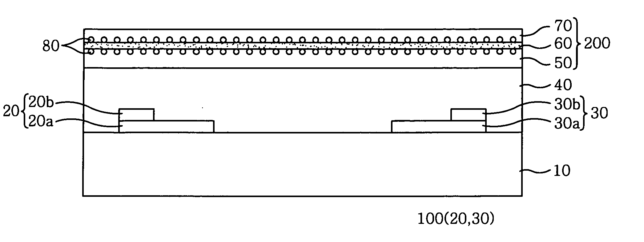
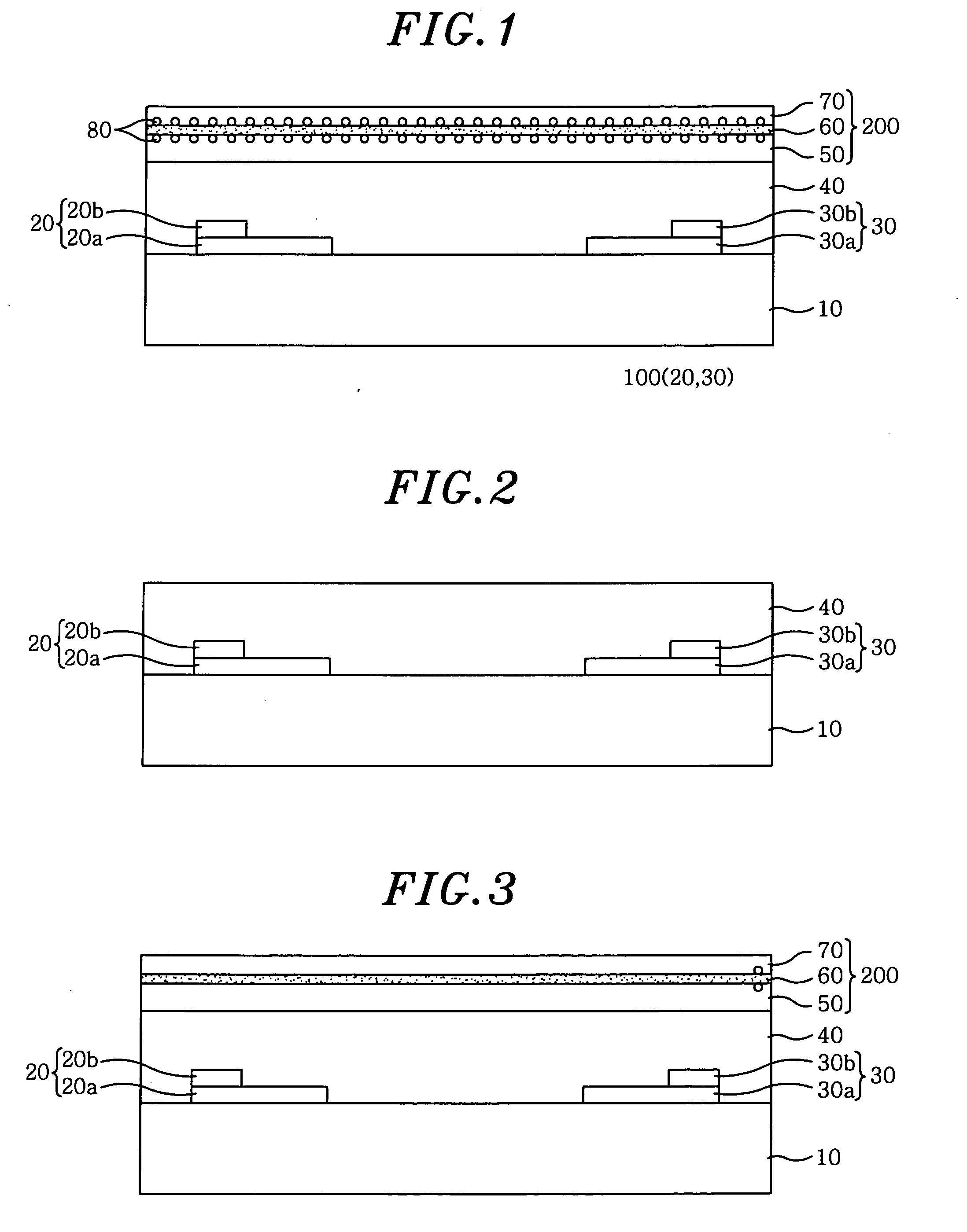
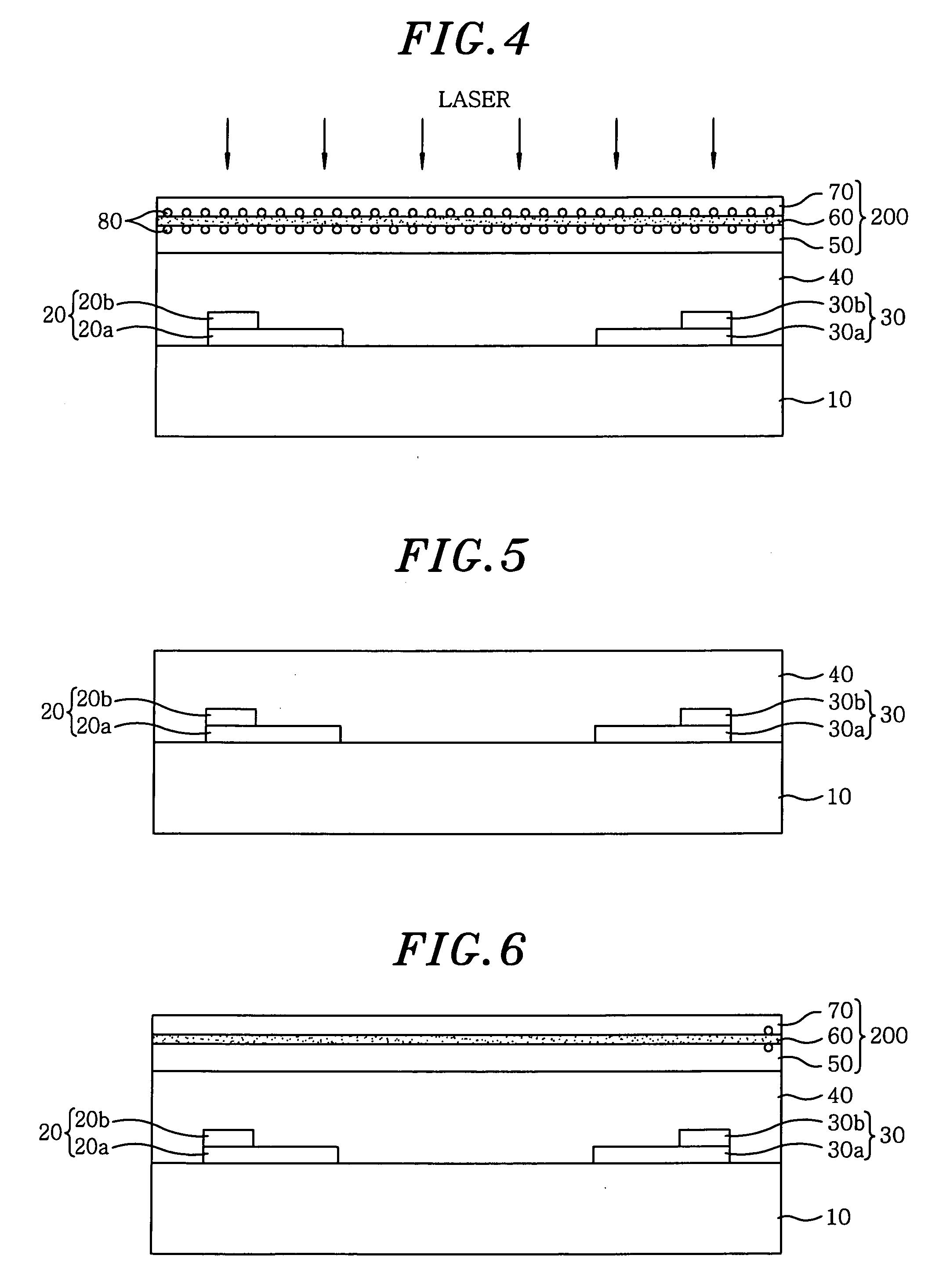
[0028]FIG. 1 is a cross-sectional view illustrating a front plate of a plasma display panel in accordance with an exemplary embodiment.

[0029]Referring to FIG. 1, a scan electrode 20 and a display electrode 30 are disposed on a glass substrate 10 to be spaced apart from each other by a predetermined distance as a discharge sustaining electrode 100. the scan electrode 20 includes a transparent electrode 20a and a bus electrode 20b disposed on a portion of the top surface of the transparent electrode 20a, and the display electrode 30 includes a transparent electrode 30a and a bus electrode 30b disposed on a portion of the top surface of the transparent electrode 30a. The transparent electrodes 20a and 30a are formed of a transparent conductive material, e.g., indium tin oxide (ITO), indium zinc oxide (IZO), etc., considering their transmittance. In order to compensate high re...


PUM

PropertyMeasurementUnit
band gap energyaaaaaaaaaa
wavelengthaaaaaaaaaa
thicknessaaaaaaaaaa

Abstract

A passivation film and a method of forming the same are provided, the passivation film being used in a plasma display panel etc. In the passivation film, a first MgO layer, an intervening layer, and a second MgO layer are laminated and a laser is then irradiated to oxidize the intervening layer. Simultaneously, defects are formed at the interfaces of the first and second MgO layers. Accordingly, a plasma discharge firing voltage greatly decreases, and the total power consumption of the plasma display panel is significantly reduced.

Description

[0001]This application is a Continuation-In-Part Application of PCT International Application No. PCT / KR2007 / 005363 filed on Oct. 30, 2007, which designated the United States.FIELD OF THE INVENTION[0002]The present invention relates to a passivation film and a method of forming the same, and more particularly, to a passivation film, which can improve discharge characteristic of an MgO layer widely used in a plasma display panel (PDP), and a method of forming the same.BACKGROUND OF THE INVENTION[0003]Generally, plasma display panels are display devices in which ultraviolet (UV) light generated by gas discharge within discharge cells excites phosphors to display images. Plasma display panels are considered as next generation flat panel display devices because they can realize large-sized high-resolution display screens.[0004]A plasma display panel configuration including a rear plate provided with an address electrode, a barrier rib, and a phosphor layer corresponding to each discharg...

Claims


Application Information

Patent Timeline
Patent Type & Authority Applications(United States)
IPC IPC(8): H01L21/30B32B9/00B05D3/06
CPCC23C26/00C23C28/04H01J9/02C23C28/345H01J11/40C23C28/322H01J11/12H01J9/20
Inventor LEE, JONG LAMYU, HAK KI
Owner LG ELECTRONICS INC
Why Eureka
Try Eureka