Plasma display panel

a technology of display panel and plasma, which is applied in the direction of gas discharge vessel/container, discharge tube/container, and address electrode, etc., can solve the problems of discharge firing voltage, cost of manufacturing pdp, and significant loss of input energy applied to sustain electrode and scan electrode, so as to reduce discharge firing voltage and increase luminous efficiency

Inactive Publication Date: 2006-05-18
SAMSUNG SDI CO LTD
View PDF9 Cites 3 Cited by
  • Summary
  • Abstract
  • Description
  • Claims
  • Application Information

AI Technical Summary

Benefits of technology

[0015] The present invention provides a plasma display panel which can increase luminous efficiency while reducing a discharge firing voltage by providing an opposed discharge structure.

Problems solved by technology

By these steps, an input energy applied to the sustain electrode and the scan electrode is significantly lost.
However, there is a problem in that the increasing the area or the length of the positive column region and the partial pressure of xenon (Xe) increases a discharge firing voltage and the cost of manufacturing the PDP.

Method used


Image

  • Plasma display panel
  • Plasma display panel
  • Plasma display panel

Examples


first embodiment

[0074] Hereinafter, various embodiments of the present invention will be described. Since the structures of the below-described embodiments are similar or identical to that of the first embodiment, the same parts will be omitted and only different portions will be described.

second embodiment

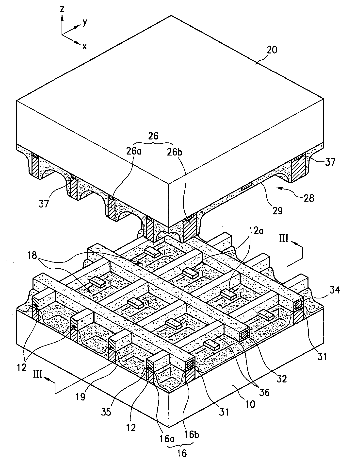
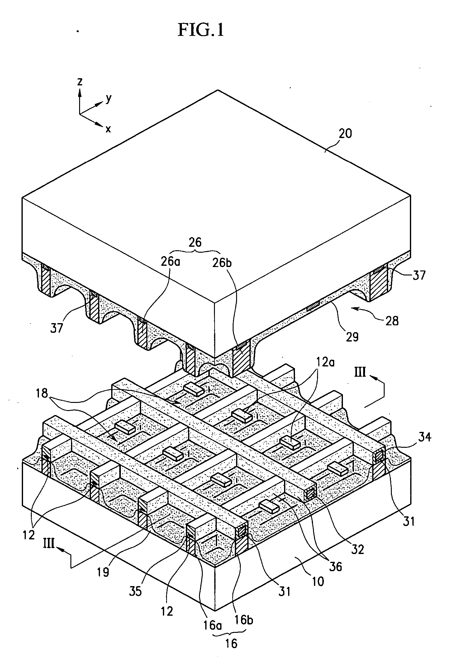
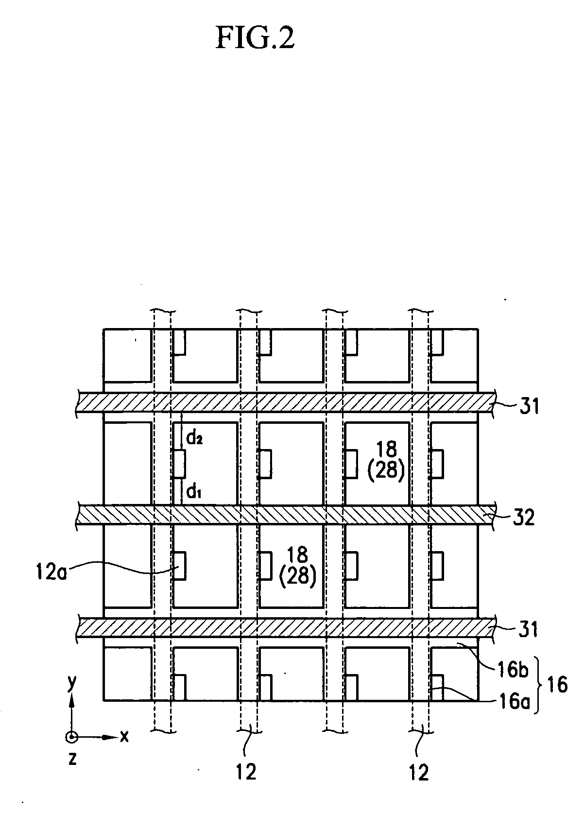
[0075]FIG. 6 illustrates the present invention. In this embodiment, the rear barrier rib 216 is composed of a first barrier rib member that is formed in a direction parallel with the address electrode 12, and the front barrier rib 226 is composed of a second barrier rib member which is formed in a direction parallel with the address electrode 12. Accordingly, the discharge cells 18 and 28 are formed in a stripe shape which is continuously connected in a direction (y-axis direction) in which the address electrode 12 extends.

[0076]FIG. 7 is a partial exploded perspective view showing a plasma display panel according to a third embodiment of the present invention. FIG. 8 is a partial plan view schematically illustrating the structure of the electrodes and the discharge cells in a plasma display panel according to the third embodiment of the present invention. FIG. 9 is a partial cross-sectional view taken along the line IX-IX in the state of assembling the plasma display panel of FIG. ...

third embodiment

[0077] In this third embodiment, protrusions 331a and 332a are provided to a sustain electrode 331 and a scan electrode 332, respectively. That is, the protrusions 331a and 332a are protruded toward the centers of the discharge cells 18 and 28. The protrusion 12a of the address electrode 12 and the protrusion 332a of the scan electrode 332 form a shorter gap and thus the address discharge is generated at a low voltage. Also, the protrusion 331a of the sustain electrode 331 and the protrusion 332a of the scan electrode 332 form a shorter gap at the beginning of the sustain discharge and thus the sustain discharge is generated at a low voltage. Also, a long gap discharge may be performed, compared with the beginning of the sustain discharge, and the sustain discharge is generated on both sides of the discharge cells 18 and 28. Accordingly, the luminous efficiency is improved.

[0078] The black layer 337 may be formed in a shape corresponding to the plane pattern of the address electrode...


PUM


Abstract

The invention provides a plasma display panel having an opposed discharge configuration that can improve luminous efficiency while reducing a discharge firing voltage. The PDP may include a first substrate separated from an opposing second substrate by a predetermined interval. A plurality of discharge cells may be defined between the substrates within this interval. Address electrodes having protrusions that protrude toward the inside of each discharge cell may extend on the first substrate along a first direction. First electrodes may be arranged on both sides of the discharge cell along a second direction crossing the first direction and may be spaced from the address electrode between the first substrate and the second substrate. Second electrodes arranged between and substantially parallel the first electrodes may pass through each discharge cell. The first and second electrodes may project away from the first substrate and in a direction toward the second substrate.

Description

CROSS REFERENCE TO RELATED APPLICATIONS [0001] This application claims priority to and the benefit of Korean Patent Application No. 10-2004-0093921, filed on Nov. 17, 2004 in the Korean Intellectual Property Office, the entire content of which is incorporated herein by referenceBACKGROUND OF THE INVENTION [0002] 1.Field of the Invention [0003] The present invention relates to a plasma display panel, and more particularly, to a plasma display panel which can improve luminous efficiency while reducing a discharge firing voltage. [0004] 1.Discussion of the Background [0005] In a plasma display panel (“PDP”), there is a three-electrode surface discharge type structure. The three-electrode surface discharge type structure includes substrate including sustain electrodes and scan electrodes which are formed on the same surface and another substrate which is spaced therefrom at a predetermined distance and has address electrodes arranged in perpendicular to the sustain electrodes and the sc...

Claims


Application Information

Patent Timeline
Patent Type & Authority Applications(United States)
IPC IPC(8): H01J17/49H01J11/12H01J11/16H01J11/22H01J11/24H01J11/26H01J11/32H01J11/34H01J11/36H01J11/40H01J11/42H01J11/44
CPCH01J11/16H01J11/24H01J11/26H01J2211/245H01J2211/265H01J2211/361H01J11/38H01J11/40
Inventor HUR, MINCHOI, HOON-YOUNGCHOI, YOUNG-DOMIZUTA, TAKAHISA
Owner SAMSUNG SDI CO LTD
Why Eureka
Try Eureka