Method and apparatus for optimized parallel testing and access of electronic circuits

a technology of parallel testing and access, applied in the field of scan-based testing of integrated circuits, printed circuit boards, systems, etc., can solve the problems of limited ate testing to a single uut, and the scalability of traditional ate is often impractical

Inactive Publication Date: 2006-05-18
INTELLITECH INC
View PDF15 Cites 50 Cited by
  • Summary
  • Abstract
  • Description
  • Claims
  • Application Information

AI Technical Summary

Benefits of technology

[0023] In accordance with the present invention, a Parallel Test Architecture (PTA) is provided that facilitates concurrent access to multiple electronic circuits (i.e., simultaneously) for optimized testing and / or debugging purposes, or for the configuration of programmable circuits. In one embodiment, the PTA includes a communications path, a primary test controller, and one or more local test controllers. The primary controller is configured to provide predetermined stimulus, expected, and mask data to the local controllers over the communications path. The local controllers are configured to apply the stimulus data to the electronic circuits, to receive resultant data generated by the circuits in response to the stimulus data, and to verify the resultant data locally against the expected data substantially concurrently. When the communications path is implemented as an IEEE 1149.1 (JTAG) test bus, the primary controller can provide the expected and mask data to the local controllers over the TDO and TRSTN lines while the TAP controllers of the electronic circuits are in the Shift-IR or Shift-DR state to enable concurrent testing over a traditional five wire multi-drop IEEE 1149.1 test bus.
[0025] The presently disclosed parallel test architecture reduces costs associated with testing of electronic circuits and configurations of programmable logic devices and memories. With the PTA, the cost of Automatic Test Equipment (ATE) is greatly reduced, as the test apparatus required to control the PTA can be implemented by a low-cost system such as a Personal Computer (PC) or a Unix-based workstation instead of a full-function ATE. In addition, costs are reduced because the PTA can test or program multiple circuits in parallel, thereby minimizing testing and programming times. The PTA also provides for ease of scalability over traditional ATE. Typically, ATE is limited to testing a single UUT or only a few devices in parallel. Further, scalability of traditional ATE is often impractical, as it is costly to add resources (e.g., tester channels and vector memory) or utilize additional ATE to provide increased “parallel” testing of multiple UUTs.
[0026] The PTA is configured to provide true parallel testing of multiple UUTs. It is capable of testing or verifying a number of UUTs simultaneously, i.e., in parallel, rather than one at a time. With the PTA, the speed-up in test time over that of serial testing is equal to the number of UUTs that are connected and tested in parallel. The PTA solves numerous problems of conventional test architectures such as the problem of requiring separate TDO lines for each UUT. This makes it possible for PTA to be practically implemented and used for a variety of applications. For instance, the PTA can be implemented separately from the devices or UUTs, or it can be implemented together with the UUTs as a part of a final system configuration. For example, in the case of chip testing at wafer probe, the PTA can be implemented as part of a tester or probe interface card. Further, the PTA can be implemented on each of the PCBs that plug into a system backplane. It is also possible to implement the PTA within an IC, e.g., to provide parallel test where the UUTs are embedded cores within an SoC.
[0028] The presently disclosed parallel test architecture provides a low-cost optimal solution to parallel testing of electronic circuits and / or configuration of programmable circuits. It can be implemented in a variety of ways appropriate to the application use. Further, the PTA supports any number of DFT methodologies for testing of the UUT, e.g., Boundary Scan, internal scan, and BIST.

Problems solved by technology

Typically, ATE is limited to testing a single UUT or only a few devices in parallel.
Further, scalability of traditional ATE is often impractical, as it is costly to add resources (e.g., tester channels and vector memory) or utilize additional ATE to provide increased “parallel” testing of multiple UUTs.

Method used


Image

  • Method and apparatus for optimized parallel testing and access of electronic circuits
  • Method and apparatus for optimized parallel testing and access of electronic circuits
  • Method and apparatus for optimized parallel testing and access of electronic circuits

Examples


Embodiment Construction

[0050] U.S. patent application Ser. No. 10 / 119,060 filed Apr. 9, 2002 entitled METHOD AND APPARATUS FOR OPTIMIZED PARALLEL TESTING AND ACCESS OF ELECTRONIC CIRCUITS, and U.S. Provisional Patent Application No. 60 / 303,052 filed Jul. 5, 2001 entitled METHOD AND APPARATUS FOR OPTIMIZED PARALLEL TESTING AND ACCESS OF ELECTRONIC CIRCUITS, are incorporated herein by reference.

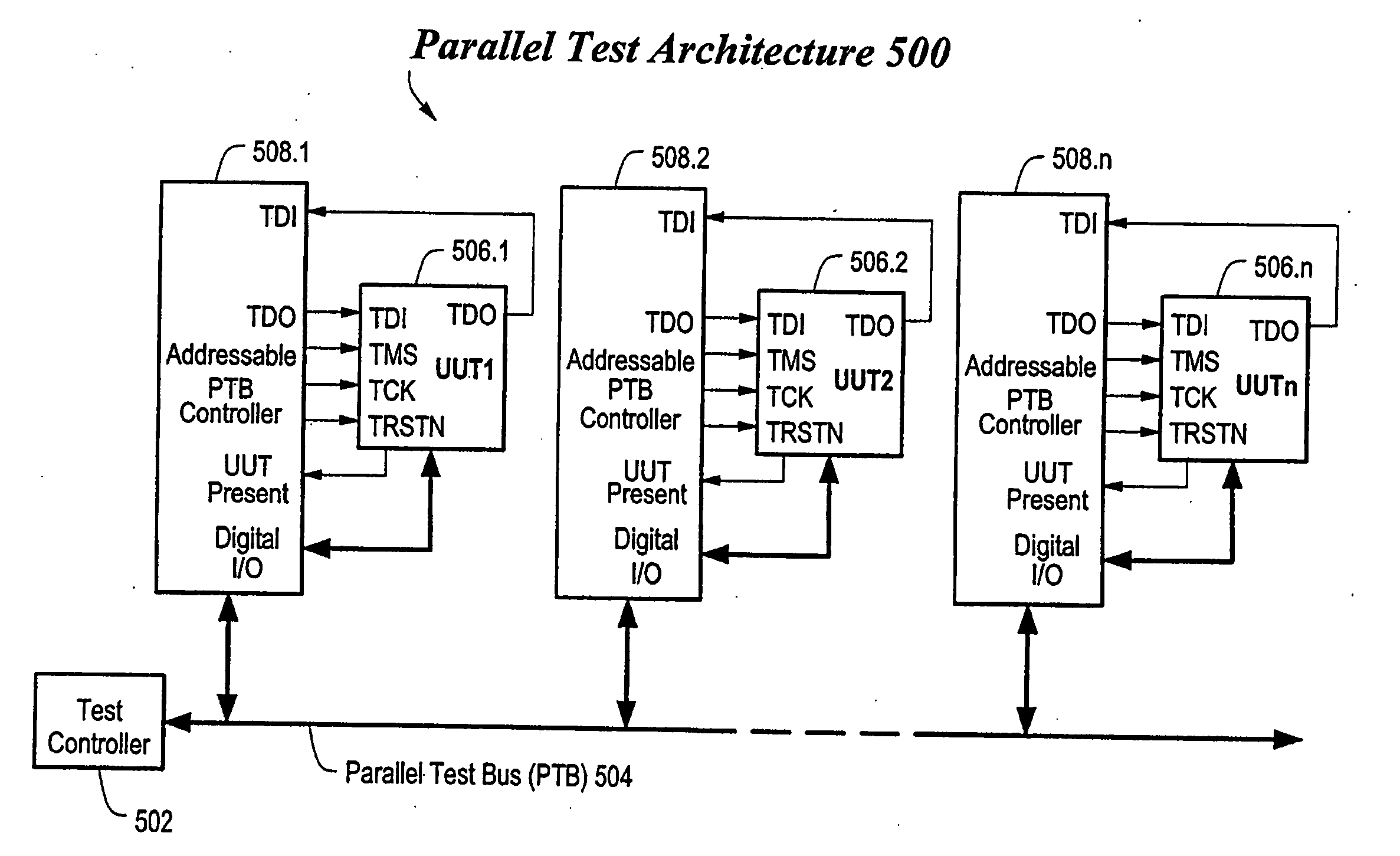
[0051]FIG. 5 depicts an illustrative embodiment of a Parallel Test Architecture (PTA) 500, in accordance with the present invention. In the illustrated embodiment, a test controller 502 is connected to a Parallel Test Bus (PTB) 504. For example, the test controller 502 may be either a separate external test controller or an embedded master controller, e.g., embedded with the system including Units Under Test (UUTs) 506.1-506.n. The test controller 502 is configured to communicate over the PTB 504 using the protocol of the PTA 500, which is described below. In this illustrated embodiment, the UUTs 506.1-506.n are con...


PUM


Abstract

A Parallel Test Architecture (PTA) is provided that facilitates concurrent test, debug or programmable configuration of multiple electronic circuits (i.e., simultaneously). The PTA includes a communications path, a primary test controller, and a number of local test controllers. The primary controller provides stimulus, expected, and mask data to the local controllers over the communications path. The local controllers apply the stimulus data to the electronic circuits, receive resultant data generated by the circuits in response to the stimulus data, and locally verify the resultant data against the expected data substantially concurrently. When the communications path is implemented as an IEEE 1149.1 (JTAG) test bus, the primary controller can provide the expected and mask data to the local controllers over the TDO and TRSTN lines while the TAP controllers of the electronic circuits are in the Shift-IR or Shift-DR state to enable concurrent testing over a traditional five wire multi-drop IEEE 1149.1 test bus.

Description

CROSS REFERENCE TO RELATED APPLICATIONS [0001] This application is a continuation-in-part application of prior U.S. patent application Ser. No. 10 / 119,060 filed Apr. 9, 2002 entitled METHOD AND APPARATUS FOR OPTIMIZED PARALLEL TESTING AND ACCESS OF ELECTRONIC CIRCUITS, which claims benefit of U.S. Provisional Patent Application No. 60 / 303,052 filed Jul. 5, 2001 entitled METHOD AND APPARATUS FOR OPTIMIZED PARALLEL TESTING AND ACCESS OF ELECTRONIC CIRCUITS.STATEMENT REGARDING FEDERALLY SPONSORED RESEARCH OR DEVELOPMENT [0002] N / A BACKGROUND OF THE INVENTION [0003] The present invention relates generally to scan-based testing of integrated circuits, printed circuit boards, and systems, and more particularly to a method and apparatus for accessing multiple such electronic circuits within a system and for optimized testing of multiple such electronic circuits in parallel. [0004] Scan-based testing is frequently employed during the development and manufacturing of electronic components (e...

Claims


Application Information

Patent Timeline
Patent Type & Authority Applications(United States)
IPC IPC(8): G01R31/28G06F11/00G01R31/3185G06F11/22G11C29/56
CPCG01R31/318516G01R31/318555G11C2029/2602G11C29/56G01R31/318563G01R31/28
Inventor RICCHETTI, MICHAELCLARK, CHRISTOPHER J.
Owner INTELLITECH INC
Why Eureka
Try Eureka