Native incorporation of RF ID technology for the tracking of electronic circuitry

a technology of electronic circuitry and incorporation technology, which is applied in the direction of transmission, basic electric elements, solid-state devices, etc., can solve the problems of small and limited amount, and the integrated circuit device and information unit do not meet the ieee family of standards, and achieve a broader commercial and industrial utility

Inactive Publication Date: 2006-06-29
IBM CORP
View PDF8 Cites 2 Cited by
  • Summary
  • Abstract
  • Description
  • Claims
  • Application Information

AI Technical Summary

Benefits of technology

[0008] The present invention provides RF ID circuitry on each chip to be identified, and the RF ID circuitry is fabricated as an integral part of the manufacturing process for that chip. This provides a very low cost method of chip identification, reducing identification errors, and eliminating the need and associated expense for other forms of identification, and enabling new identification capabilities. The RF ID circuitry is fabricated in compliance with IEEE family of standards 802, such that the invention is useful for a very broad range of applications that are enabled because of compliance with the IEEE family of standards 802.
[0010] Compliance with the IEEE family of standards 802 enables the present invention to have a much broader commercial and industrial utility than the narrow field of theft detection and prevention as disclosed by U.S. Pat. No. 6,525,410, and can be utilized to identify a chip in many different environments and at many different stages, from its initial fabrication through the manufacturers supply chain to the consumer, and even during usage by a consumer. Compliance with the IEEE family of standards 802 and Bluetooth technology enable the chip to be identified in many different environments and at any of the stages of its fabrication, inspection, distribution and commercial usage.

Problems solved by technology

A major drawback of these identification methods is that they can place only a fairly small and limited amount of identifying information on each chip / wafer, and moreover an optical reading capability is required to access that limited amount of information.
Moreover, the integrated circuit device and information unit do not comply with the IEEE family of standards 802.

Method used


Image

  • Native incorporation of RF ID technology for the tracking of electronic circuitry
  • Native incorporation of RF ID technology for the tracking of electronic circuitry

Examples


Embodiment Construction

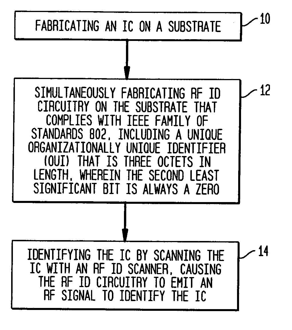
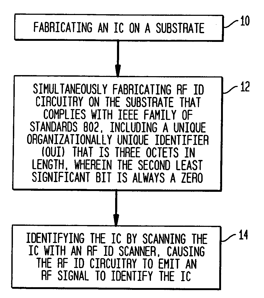
[0013] Unlike current RF ID technologies that attach a stand-alone identification tag to the object to be identified, the present invention improves on this methodology and enables the chip industry to provide an RF ID capability integral to the product. This eliminates the possibility of mislabeling a chip later in the process, and is implemented by fabricating the RF ID circuit as an integral part of each chip.

[0014] The present invention provides a method of identifying wafers and chips by fabricating each of the wafers and chips with a standard range RF ID circuit or a near range RF ID circuit that is electrically powered by RF energy irradiating the circuit from RF ID scanning equipment, as is known in the art. The identification of wafers and chips by fabricating each of the wafers and chips with an RF ID pursuant to the present invention requires only standard RF ID scanning equipment. The in-situ or intrinsically fabricated RF ID allows identification and control of wafers ...


PUM


Abstract

RF ID transmitter circuits are integrated into semiconductor chips during fabrication of the regular integrated circuits therein for providing identification capabilities for the semiconductor chips that comply with the IEEE family of standards 802. The RF ID transmitter circuit enables each chip to be identified in many different environments and at any of the stages after its fabrication, including inspection, distribution and commercial usage of the chip.

Description

BACKGROUND [0001] 1. Field of the Invention [0002] The present invention relates generally to the manufacture of semiconductor wafers, chips and components, and more particularly pertains to a novel system and process for integrating RF ID transmitter circuits into semiconductor chips during their fabrication for providing identification capabilities for the semiconductor chips that comply with the IEEE family of standards 802. The RF ID transmitter circuit enables each chip to be identified in many different environments and at any of the stages after its fabrication, including inspection, distribution and commercial usage of the chip. [0003] 2. Description of the Prior Art [0004] In the present state of the art, semiconductor chips and wafers are identified either by marking the container they are placed in (as in speed sort bins) or by physically marking each chip or wafer. These markings include both alphanumeric markings and bar codes. A major drawback of these identification m...

Claims


Application Information

Patent Timeline
Patent Type & Authority Applications(United States)
IPC IPC(8): H04B7/00H01L21/50H01L23/34
CPCH01L23/544H01L2223/5444H01L2924/0002H01L2924/00
Inventor WALKO, JOSEPH P.
Owner IBM CORP
Why Eureka
Try Eureka