Optical semiconductor unit

Active Publication Date: 2006-07-13
ROHM CO LTD
View PDF3 Cites 34 Cited by
  • Summary
  • Abstract
  • Description
  • Claims
  • Application Information

AI Technical Summary

Benefits of technology

[0010] The present invention has been conceived under the circumstances described above. It is therefore an object of the present

Problems solved by technology

However, the optical semiconductor device B has the following problems.
However, since the dimension of the optical semiconductor device B increases by as much as the projecting amount of the convex lens 131 as noted abo

Method used


Image

  • Optical semiconductor unit
  • Optical semiconductor unit
  • Optical semiconductor unit

Examples


first embodiment

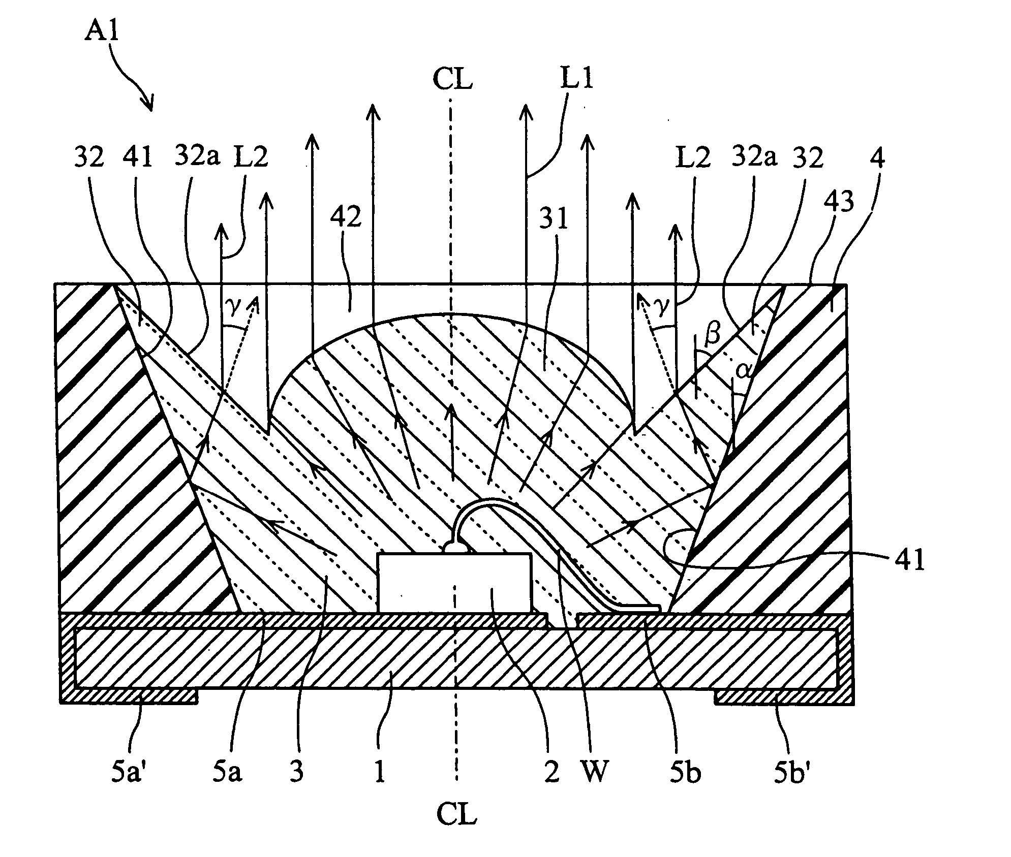
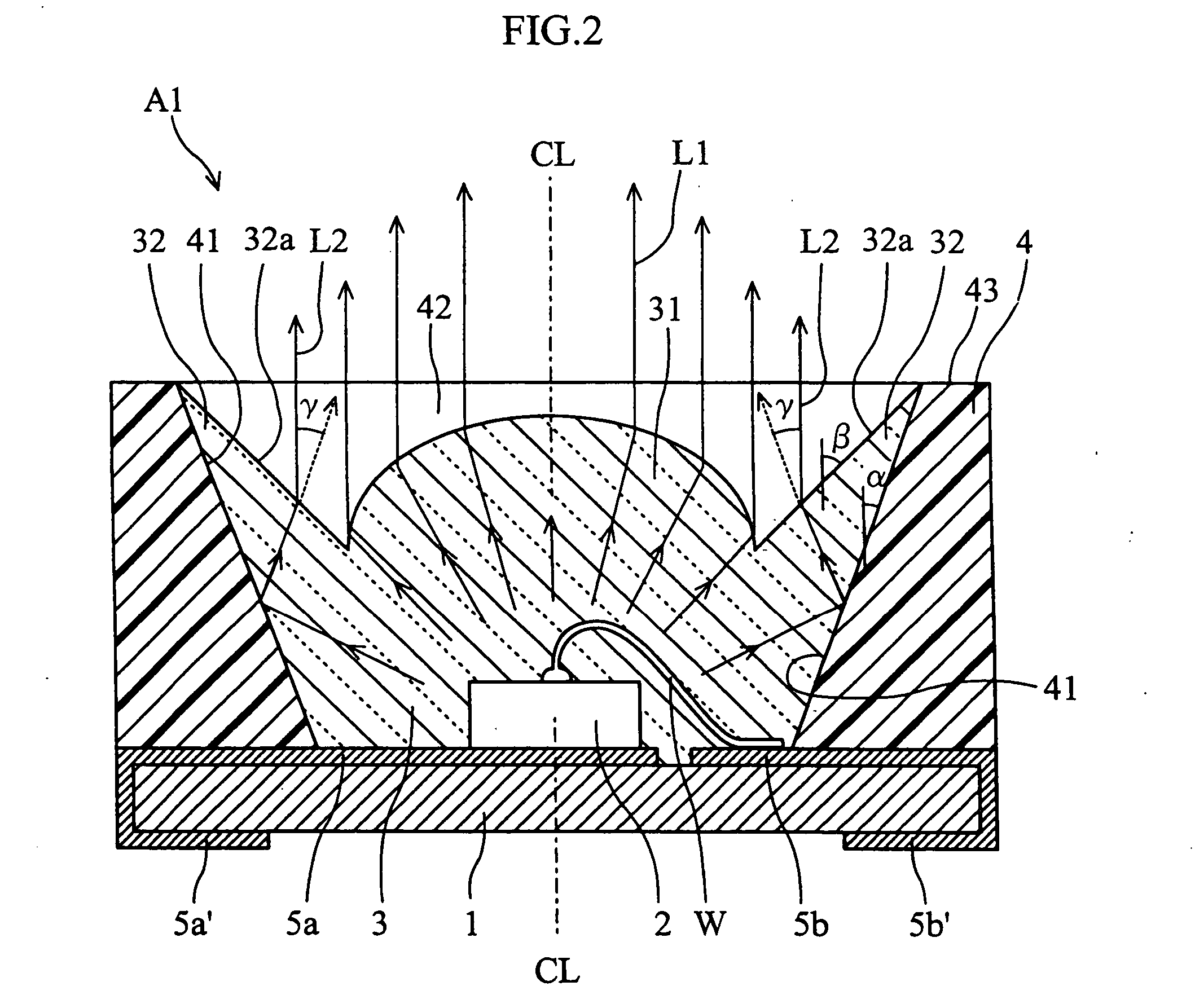
[0027]FIGS. 1 and 2 show an optical semiconductor device according to the present invention. The illustrated optical semiconductor device A1 includes a rectangular insulating substrate 1, an LED chip 2, a light permeable member 3 and a reflector 4.

[0028] The substrate 1 is made of a glass-fiber-reinforced epoxy resin, for example. The LED chip 2, the light permeable member 3 and the reflector 4 are mounted on the upper surface of the substrate 1. The LED chip 2 has an upper surface and a lower surface respectively formed with electrodes. The LED chip 2 is bonded to a first conductor portion 5a provided on the substrate 1. By this bonding, the electrode on the lower surface of the chip 2 is electrically connected to the first conductor portion 5a. The electrode on the upper surface of the chip 2 is electrically connected, via a wire W, to a second conductor portion 5b provided on the substrate 1. The first and the second conductor portions 5a, 5b extend from the upper surface up to t...

second embodiment

[0040]FIG. 4 shows the basic structure of an optical semiconductor device A2 according to the present invention. In the optical semiconductor device A2, the extension 32 of the light permeable member 3 has a front end surface (upper surface) 32b which is flush with the upper surface 43 of the reflector 4. The inclination angle β of the light emitting surface 32a of the extension 32 is equal (or generally equal) to the inclination angle α of the reflecting surface 41. Therefore, the light emitting surface 32a is parallel to the reflecting surface 41. With such a structure again, the light reflected by the reflecting surface 41 can be emitted to the outside while undergoing refraction at the light emitting surface 32a. While the light traveling generally vertically from the downside can pass through the front end surface 32b to the upside, the light impinging on the front end surface at an incidence angle which is larger than a predetermined total reflection critical angle is totally ...

third embodiment

[0042]FIG. 5 shows an optical semiconductor device A3 according to the present invention. In the optical semiconductor device A3, the light emitting surface 32a of the extension 32 is convexly curved. With the curved light emitting surface 32a, the proportion of light traveling from the reflecting surface 41 and totally reflected by the light emitting surface 32a can be made smaller than when the light emitting surface is flat. Thus, the amount of light emitted through the light emitting surface 32a can be increased.


PUM


Abstract

An optical semiconductor device includes an optical semiconductor chip, a light permeable member covering the chip, and a reflector formed with an accommodation space for accommodating the light permeable member. The light permeable member includes a convex lens for converging light emitted from the optical semiconductor chip. The reflector includes a reflecting surface for reflecting light emitted from the optical semiconductor chip. At least part of the convex lens is located within the accommodation space of the reflector. The light permeable member includes an extension engaging and extending along the reflecting surface. The extension includes a light emitting surface surrounding the convex lens.

Description

BACKGROUND OF THE INVENTION [0001] 1. Field of the Invention [0002] The present invention generally relates to an optical semiconductor device utilizing an optical semiconductor chip such as an LED chip. [0003] 2. Description of the Related Art [0004] A light emitting diode (LED) has advantages such as small power consumption, small size and long lifetime. Therefore, an optical semiconductor device utilizing an LED chip is widely used as a light source in various fields. Examples of such optical semiconductor device are disclosed in JP-A-11-345912 and JP-A-2000-183407. In these prior art devices, a convex lens or a reflector is provided to enhance the directivity of light or increase the brightness. [0005]FIG. 7 shows an example of optical semiconductor device as a related art. In the illustrated semiconductor device B, an LED chip 102 mounted on a substrate 101 is covered with a light permeable member 103. The light permeable member 103 has an upper portion formed with a convex len...

Claims


Application Information

Patent Timeline
IPC IPC(8): H01L31/109H01L33/54H01L33/56H01L33/62
CPCH01L33/54H01L2224/48465H01L2224/48091H01L2924/00H01L2924/00014
Inventor ISOKAWA, SHINJI
Owner ROHM CO LTD
Why Eureka
Try Eureka