Stacked semiconductor package having interposing print circuit board
- Summary
- Abstract
- Description
- Claims
- Application Information
AI Technical Summary
Problems solved by technology
Method used
Image

Examples
Embodiment Construction
[0024] The present invention will now be described more fully with reference to the accompanying drawings, in which example embodiments of the present invention are shown. However, the present invention should not be construed as being limited to the example embodiments set forth herein; rather, these example embodiments are provided as working examples.
[0025] Throughout the specification, designation numerals, for example, “first,”“second,” and “third” are used. The designation numerals are not used to limit or specify a specific element or method; but rather, the designation numerals are used to distinguish one element from another element for explanation purposes.
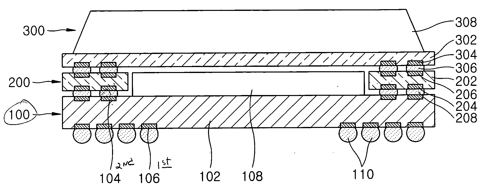
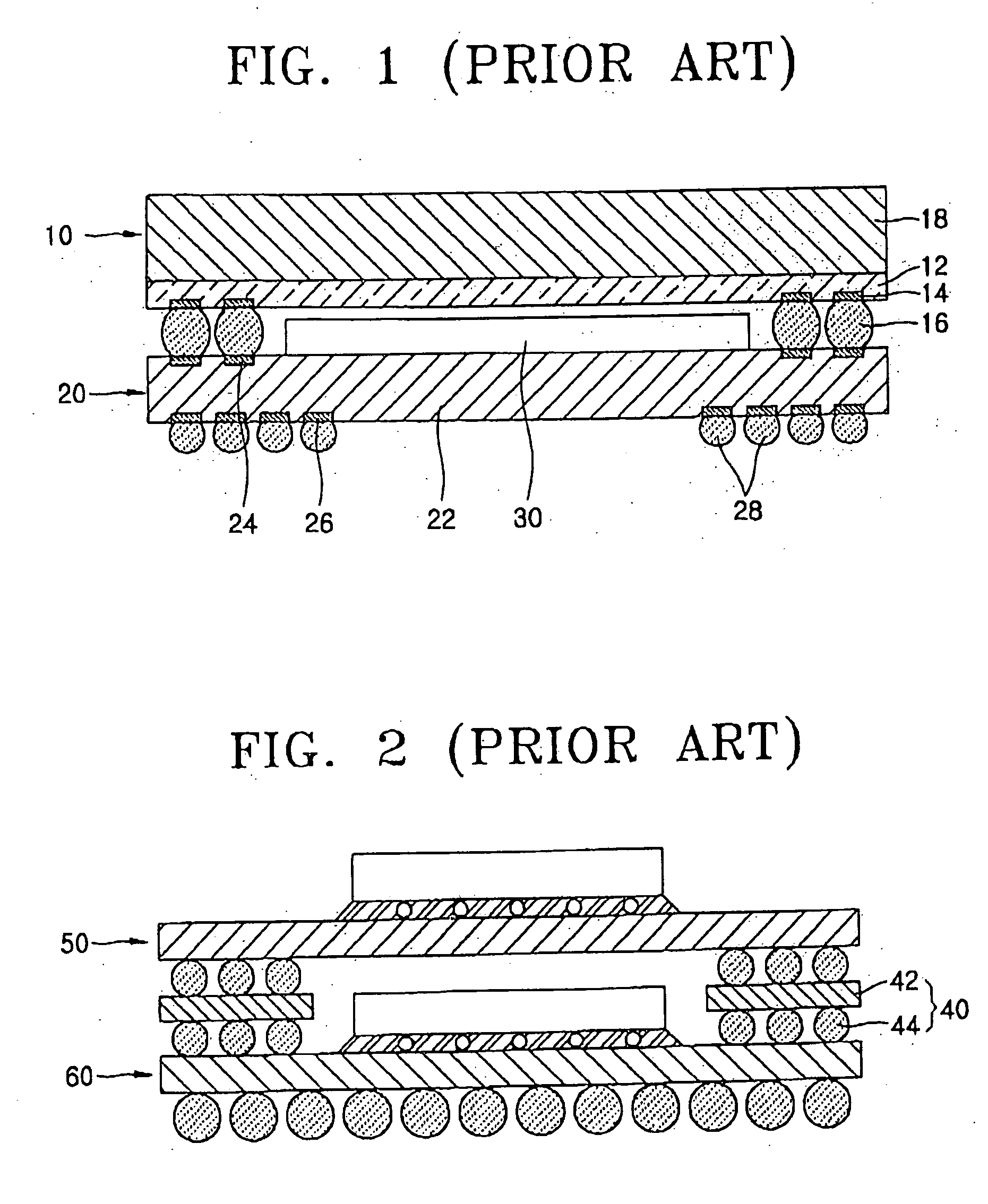
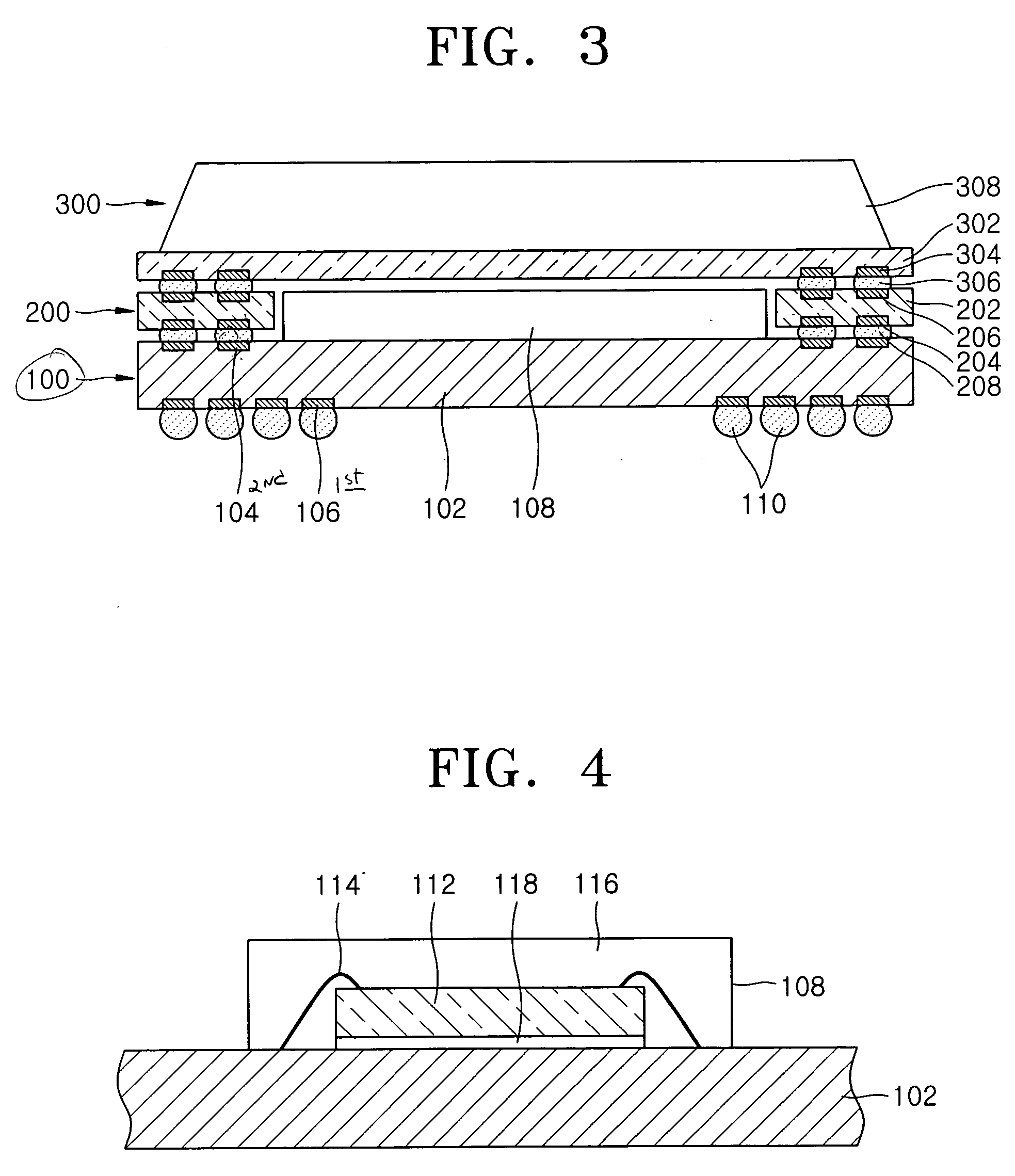
[0026]FIG. 3 is a cross-sectional view illustrating a stacked semiconductor package having an interposing print circuit board according to an embodiment of the present invention. Referring to FIG. 3, a stacked semiconductor package may include a first semiconductor package 100, a package connector 200, and a second sem...
PUM
 Abstract
Description
Claims
Application Information
 - R&D Engineer
- R&D Manager
- IP Professional
- Industry Leading Data Capabilities
- Powerful AI technology
- Patent DNA Extraction
Browse by: Latest US Patents, China's latest patents, Technical Efficacy Thesaurus, Application Domain, Technology Topic.
© 2024 PatSnap. All rights reserved.Legal|Privacy policy|Modern Slavery Act Transparency Statement|Sitemap