Complimentary metal oxide silicon low voltage positive emitter coupled logic buffer

a technology of low-voltage positive and coupled logic, which is applied in the field of buffers, can solve the problems of difficult implementation of low-voltage positive emitter coupled logic (lv-pecl) buffers, inability to implement pecl logic definitions in inability to meet the physical characteristics of mosfet devices at all, so as to achieve high-frequency switching capabilities

Active Publication Date: 2006-07-20
MICROCHIP TECH INC
View PDF3 Cites 4 Cited by
  • Summary
  • Abstract
  • Description
  • Claims
  • Application Information

AI Technical Summary

Benefits of technology

[0015] The present invention provides a LV-PECL buffer than enjoys the benefits and a

Problems solved by technology

Low-Voltage Positive Emitter Coupled Logic (LV-PECL) buffers are notorious for their difficult implementation in a complimentary metal oxide silicon (CMOS) process.
However, the physical characteristics of MOSFET devices do not fit such PECL logic definition at all.
Therefore, implementation of PECL logic in a CMOS process has traditionally been unsuccessful or at best unsatisfactory.
Additionally, with the evo

Method used


Image

  • Complimentary metal oxide silicon low voltage positive emitter coupled logic buffer
  • Complimentary metal oxide silicon low voltage positive emitter coupled logic buffer
  • Complimentary metal oxide silicon low voltage positive emitter coupled logic buffer

Examples


Embodiment Construction

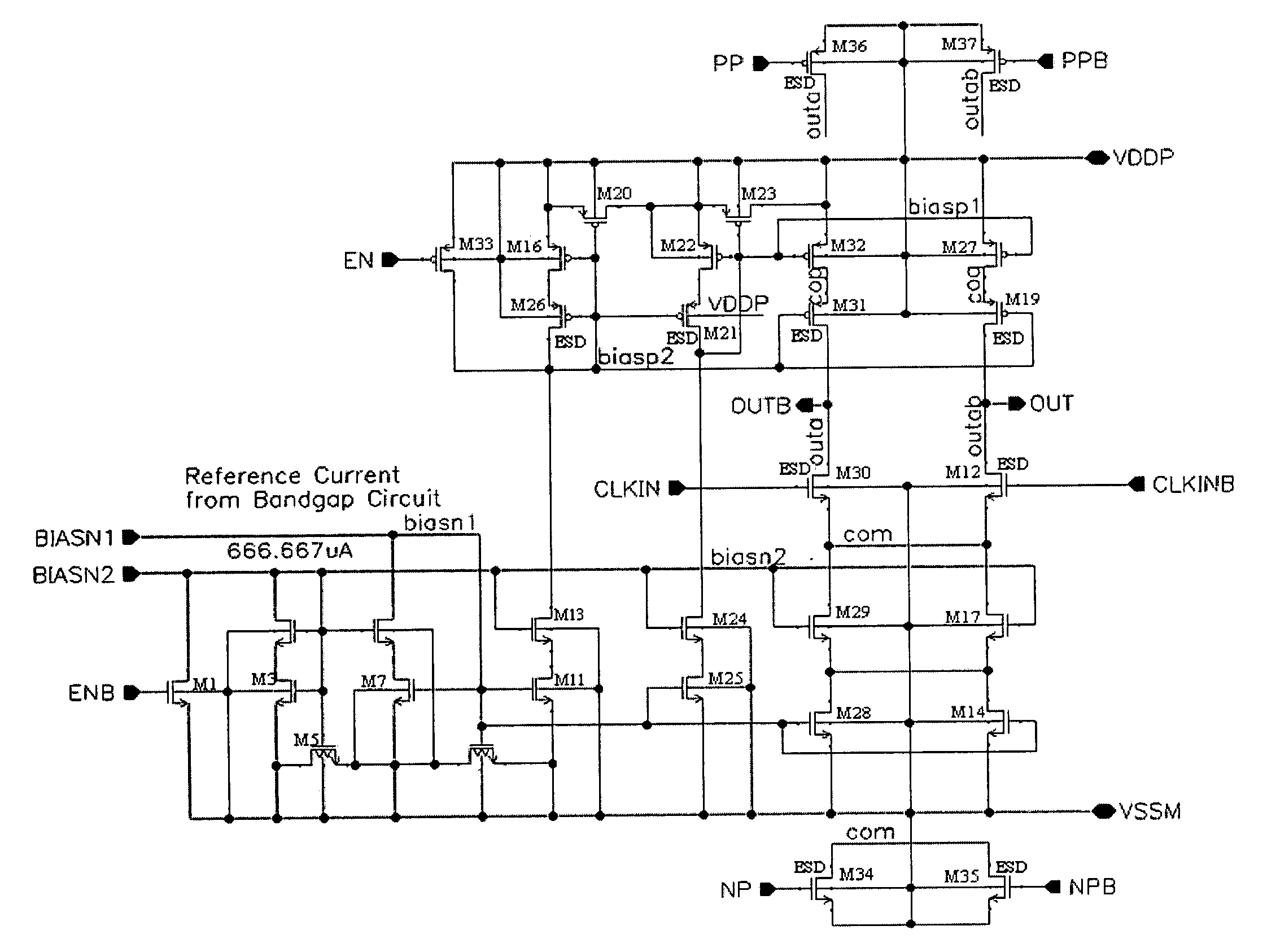
[0031] Reference will now be made in detail to the preferred embodiments of the present invention, examples of which are illustrated in the accompanying drawings. Wherever possible, the same reference numbers are used in the drawings and the description to refer to the same or like parts.

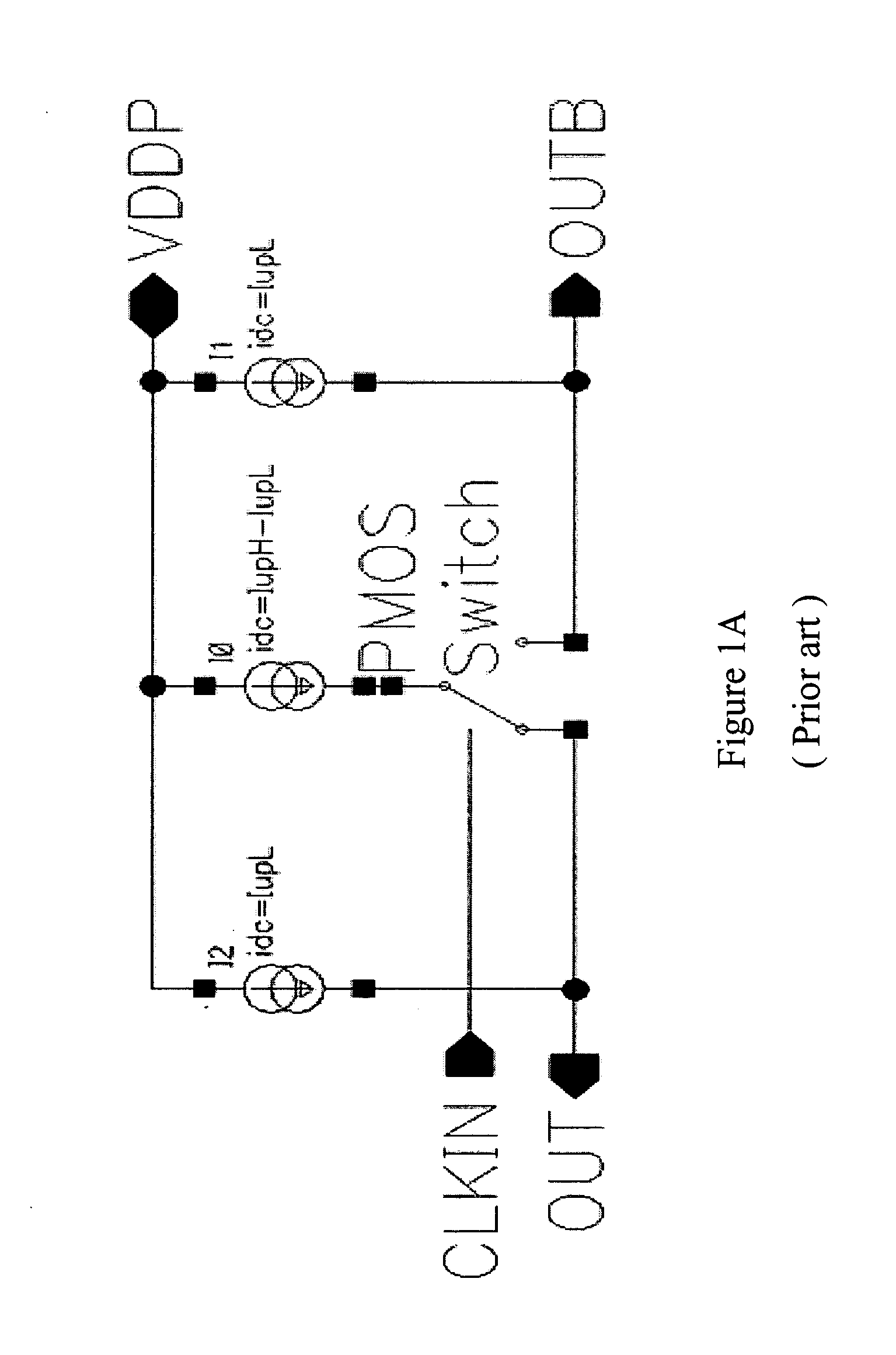
[0032] Refer to FIG. 2A, which is an amplifier utilizing an N-MOS switch according to an embodiment of the present invention.

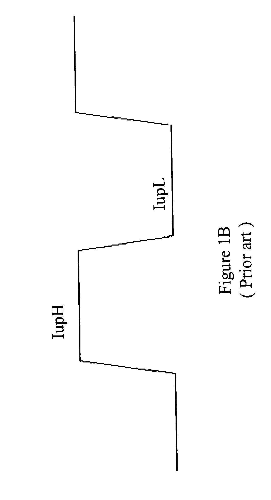
[0033] As shown in FIG. 2A, the amplifier comprises a clock input CLKIN, a first output OUT, a second output OUTB, a first voltage VDDP, a second voltage VSSM, an NMOS switch, and five current sources 13, 14, 15, 16, 17.

[0034] Current sources 15 and 14 are connected between VDDP and OUT. Current sources 13 and 16 are connected between VDDP and OUTB. OUTB is connected to one node of the NMOS Switch and OUT is connected to the other node of the NMOS Switch. Current source 17 is connected between the non-switching node of the NMOS Switch and VSSM. The clock input CLKIN control...


PUM


Abstract

A low voltage positive emitter coupled logic (LV-PECL) buffer fabricated in the complimentary oxide metal silicon (CMOS) process. The LV-PECL buffer in CMOS is operable for a wide frequency range from DC to frequencies as high as 800 MHZ in 0.5 um process. Synchronized feedforward logic is utilized without the need for a feedback loop. N-MOSFET's, which are faster than P-MOSFET's, are used for the implementation of switched current sources. The switched current sources deliver a pull-up current variable in time and as a result have more than two values. The pull-up current is sharply increased in value during the output waveform transition times in an impulse manner.

Description

BACKGROUND OF THE INVENTION [0001] 1. Field of the Invention [0002] The present invention relates to a buffer. More specifically, the present invention discloses a low voltage positive emitter coupled logic buffer in complimentary metal oxide silicon process. [0003] 2. Description of the Prior Art [0004] Low-Voltage Positive Emitter Coupled Logic (LV-PECL) buffers are notorious for their difficult implementation in a complimentary metal oxide silicon (CMOS) process. Conventional PECL logic exactly matches the physical characteristics of Bipolar devices. However, the physical characteristics of MOSFET devices do not fit such PECL logic definition at all. Therefore, implementation of PECL logic in a CMOS process has traditionally been unsuccessful or at best unsatisfactory. [0005] Additionally, with the evolution to lower voltage power supplies and lower voltage power requirements, design of such implementations has been further complicated. [0006] Refer to FIG. 1A, which is a schemat...

Claims


Application Information

Patent Timeline
IPC IPC(8): H03K19/086
CPCH03K19/018528
Inventor GUEBELS, PIERRE PAUL
Owner MICROCHIP TECH INC
Why Eureka
Try Eureka