

Method of driving plasma display panel
- Summary
- Abstract
- Description
- Claims
- Application Information
AI Technical Summary
Benefits of technology
Problems solved by technology
Method used
Image

Examples
first embodiment
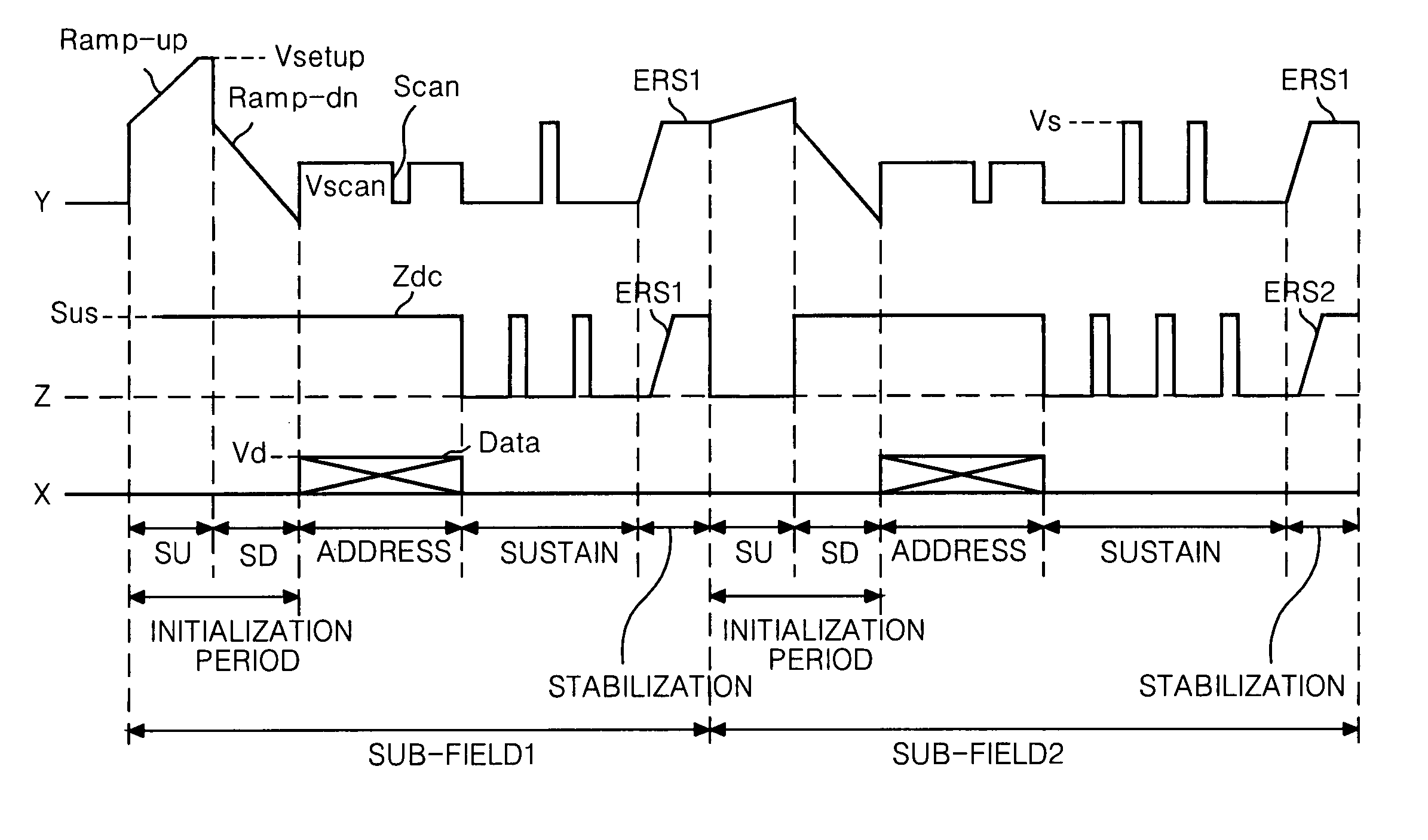
[0055]FIG. 4 is a waveform diagram in accordance with a method of driving PDP according to the present invention. As shown in FIG. 4, a scan electrode is divided into m number of groups, a strong discharge reset pulse is applied to a scan electrode belong to each group in any one frame among n number of frames 1st to Nth frame, and a weak discharge reset pulse is applied to the rest frame. Herein, the frames in which the strong reset pulse is scan electrode belong to each group are different each other.
[0056] In this case, it is preferable that a sequence of the frames in which the strong reset pulse is applied is the same as a sequence of the groups. In other words, it is preferable that the strong discharge pulse is applied to the 1st frame in the scan electrode belong to the first group, the strong discharge pulse is applied to the 2nd frame in the scan electrode belong to the second group, and the strong discharge pulse is applied to the Nth frame in the scan electrode belong to...
second embodiment
[0089]FIG. 10 shows a waveform in accordance with a method of driving PDP using a strong discharge reset pulse and a weak discharge reset pulse according to the present invention.
[0090] Referring to FIG. 10, in the method of driving the PDP according to the second embodiment of the present invention, one frame is timely divided into a plurality of sub-fields, e.x, 10 sub-fields or 12 sub-fields, to divide a scan electrode supplied to a signal into m number of blocks. For instance, When odd scan electrodes Y1, Y3, Y5, . . . are defined as a first block, even scan electrodes Y0, Y2, Y4, . . . are defined as a second block in a case that m is 2, a driving waveform including a strong discharge reset pulse is supplied to the first block during a first sub-field, and at the same time, a driving waveform including a weak discharge reset pulse is supplied to a second block. Next, while a driving waveform including a strong discharge reset pulse is supplied to the second block during a secon...
third embodiment
[0091]FIG. 11 shows a waveform in accordance with a method of driving PDP using a strong discharge reset pulse and a weak discharge reset pulse according to the present invention.
[0092] Referring to FIG. 11, in the method of driving the PDP according to the third embodiment of the present invention, one frame is timely divided into a plurality of sub-fields, e.x, 10 sub-fields or 12 sub-fields, to divide a scan electrode supplied to a signal into m number of blocks. For instance, When multiple of 3 including 0 scan electrodes Y3, Y6, . . . are defined as a first block, scan electrodes Y1, Y4, Y7, . . . are defined as a second block, and scan electrodes Y2, Y5, Y8, . . . are defined as a third block in a case that m is 3, a driving waveform including a strong discharge reset pulse is supplied to the first block during a first sub-field, and at the same time, a driving waveform including a weak discharge reset pulse is supplied to a second block and a third block. Next, while a drivin...
PUM
 Abstract
Description
Claims
Application Information