Thin film transistor array and transflective liquid crystal display panel

Inactive Publication Date: 2007-07-19
INNOLUX CORP
View PDF4 Cites 8 Cited by
  • Summary
  • Abstract
  • Description
  • Claims
  • Application Information

AI Technical Summary

Benefits of technology

[0008] The invention is directed to an array substrate , a transflective liquid crys

Problems solved by technology

Although the conventional cathode ray tube (CRT) has many advantages, the design of the electron gun renders it heavy and bulky.
Moreover, there is always some risk of hurting viewer's eyes du

Method used


Image

  • Thin film transistor array and transflective liquid crystal display panel
  • Thin film transistor array and transflective liquid crystal display panel
  • Thin film transistor array and transflective liquid crystal display panel

Examples


first embodiment

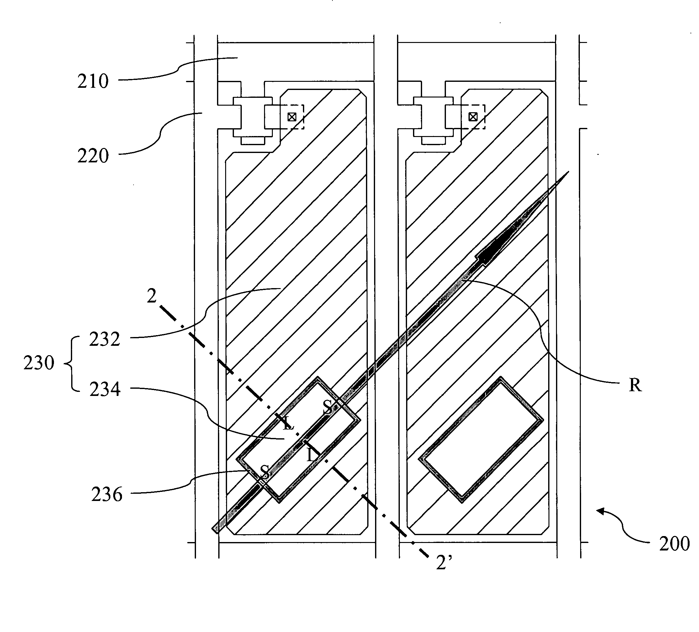
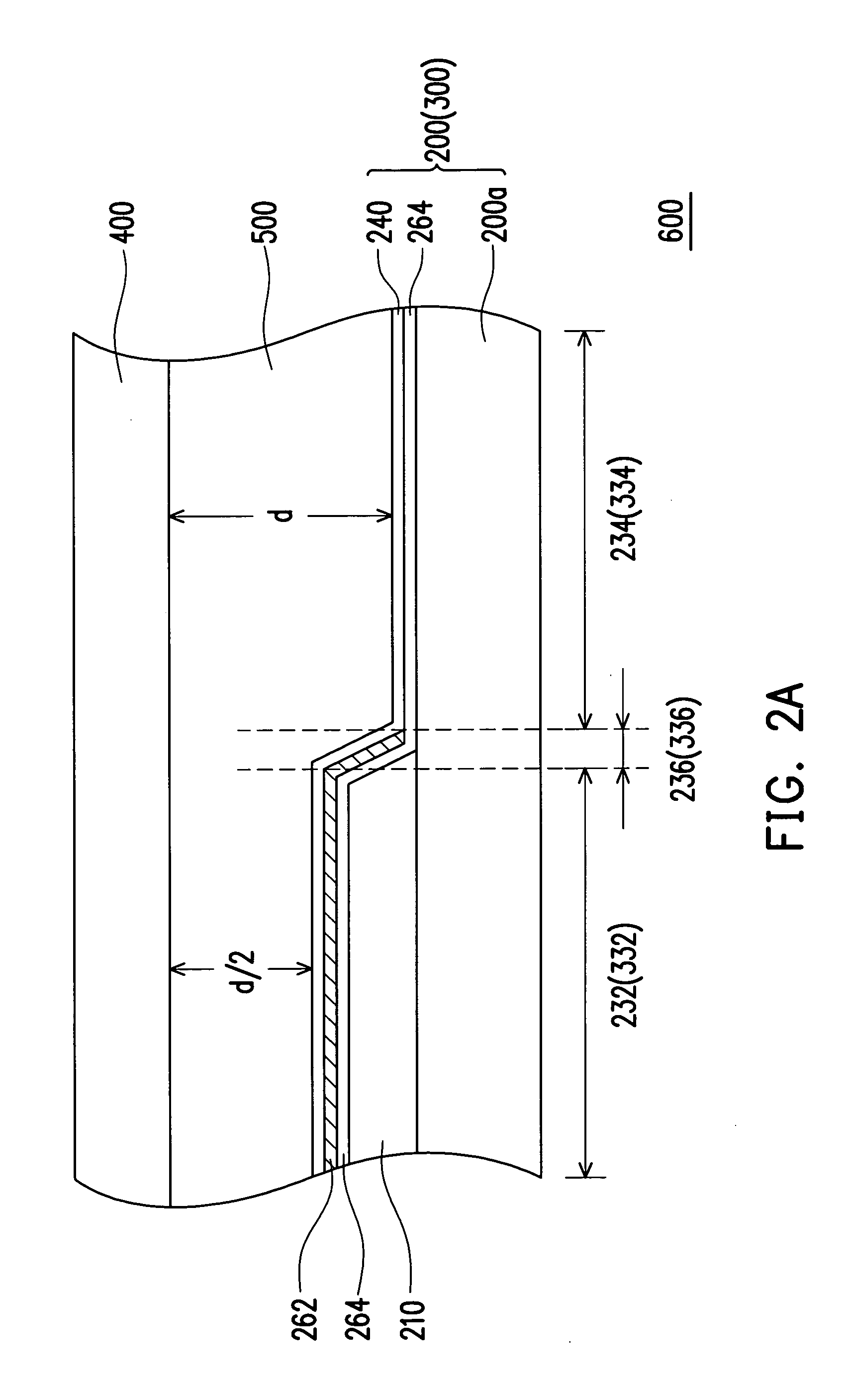
[0022]FIG. 2A is a cross-sectional view of a transflective LCD panel according to some embodiments of the present invention. Referring to FIG. 2A, the transflective liquid crystal display 600 includes a thin film transistor array 200, an opposite substrate 400 and a liquid crystal layer 500. The opposite substrate 400 is located above the thin film transistor array 200. The liquid crystal layer 500 is filled between the opposite substrate 400 and the thin film transistor array 200. In the transflective liquid crystal display 600 of the present invention, dual cell-gaps are formed between the opposite substrate 400 and the thin film transistor array 200.

[0023] More specifically, the thin film transistor array 200 includes a plurality of pixels. Each pixel of the thin film transistor array 200 includes, from the bottom to the top, a substrate 200a with a thin film transistor (not shown in FIG. 2A), a planarization layer 210 on the substrate 200a, a transparent pixel electrode 264, a ...

second embodiment

[0032]FIG. 4A˜FIG. 4C are schematic top views of a transflective thin film transistor array according to the second embodiment of the present invention. As shown in FIG. 4A˜FIG. 4C, the profile of the transmissive regions 234 is a parallelogram having a pair of first opposite sides A and a pair of second opposite sides B, for example. The length of the pair of first opposite sides A is longer than that of the pair of second opposite sides B, for example. In FIG. 4A, the pair of first opposite sides A is parallel to the rubbing direction R of the alignment film 240. In FIG. 4B and FIG. 4C, an included angle α between the pair of first opposite sides A and the rubbing direction R of the alignment film 240 (shown in FIG. 2) is smaller than 30 degree.

[0033] As shown in FIG. 4B, the included angle α between the first opposite sides A and the rubbing direction R of the alignment film 240 (shown in FIG. 2) is smaller than or equal to 30 degree. As described above, the light leakage is red...

third embodiment

[0034]FIG. 5A˜FIG. 5C and FIG. 6A˜FIG. 6B are schematic top views of a transflective thin film transistor array according to the third embodiment of the present invention. Referring to FIG. 5A˜FIG. 5C and FIG. 6A˜FIG. 6B, the profile of the transmissive regions 232 is polygon, such as pentagon (right side of FIG. 6B), hexagon (FIG. 5A˜FIG. 5C), heptagon (left side of FIG. 6B) or octagon (left side of FIG. 6A), having a pair of opposite sides X, for example.

[0035] In FIGS. 5A, 6A and 6B, the pair of opposite sides X parallel the rubbing direction R of the alignment film 240 (shown in FIG. 2). In FIG. 5B and FIG. 5C, an included angle α between the pair of opposite sides X and the rubbing direction R of the alignment film 240 (shown in FIG. 2) is smaller than or equal to 30 degree.


PUM


Abstract

An array substrate including a substrate, multiple pixels arranged in an array on the substrate, and an alignment film disposed on the pixels is provided. The pixel includes a reflective region, a transmissive region, and a transition region formed between the reflective region and the transmissive region, wherein an included angle between at least one side of the transition region and a rubbing direction of the alignment film is smaller than or equal to 30 degree. In addition, a transflective LCD including the array substrate as described above and a fabricating method of an array substrate is further provided.

Description

BACKGROUND OF THE INVENTION [0001] 1. Field of the Invention [0002] The present invention relates to a thin film transistor array (TFT array). More particularly, the present invention relates to a transflective liquid crystal display (Transflective LCD) with high contrast ratio. [0003] 2. Description of Related Art [0004] To match the life style of modern people, video or imaging equipment is becoming lighter and slimmer. Although the conventional cathode ray tube (CRT) has many advantages, the design of the electron gun renders it heavy and bulky. Moreover, there is always some risk of hurting viewer's eyes due to the production of some harmful radiation. With big leaps in the techniques in manufacturing semiconductor devices and opto-electronic devices, flat panel displays such as liquid crystal displays (LCD), organic light-emitting displays (OLED) and plasma display panels (PDP) has gradually become the mainstream display products. [0005] According to the light source used, a li...

Claims


Application Information

Patent Timeline
IPC IPC(8): G02F1/141
CPCG02F1/133784G02F1/133555
Inventor JANG, CHING-YUCHU, CHIA-CHINGCHEN, YING-YI
Owner INNOLUX CORP
Why Eureka
Try Eureka