Methods to form electronic devices and methods to form a material over a semiconductive substrate

a technology of semi-conductive substrates and electronic devices, which is applied in the direction of coatings, chemical vapor deposition coatings, capacitors, etc., can solve the problems of pin holes or other defects in the deposited layer, the thickness of the capacitor dielectric layer is smaller, and the conventional capacitor dielectric materials such as siosub>2/sub>nsub>4/sub>may become unsuitable,

Inactive Publication Date: 2006-07-27
THAKUR RANDHIR
View PDF38 Cites 3 Cited by
  • Summary
  • Abstract
  • Description
  • Claims
  • Application Information

AI Technical Summary

Problems solved by technology

As the density of DRAM cells increases, there is a continuing challenge to maintain sufficiently high storage capacitance despite decreasing cell area.
Such overall reduction in cell size drives the thickness of the capacitor dielectric layer to smaller values, and conventional capacitor dielectric materials such as SiO2 and Si3N4 might become unsuitable.
Yet processing associated with chemical vapor deposition of thin silicon nitride films in certain environments has also created other problems not directly associated with the capacitors.
Typical deposition conditions are at sub-Torr pressures and temperatures at or above 680° C., more typically above 700° C. The deposition process and the very thin nature of the typically deposited silicon nitride layer results in pin holes or other defects in the deposited layer.
However as the nitride thickness of the ONO construction over the storage node electrode fell to below 80 Angstroms, it was discovered that the underlying bulk silicon substrate was oxidizing to the point of circuit destruction.
BPSG is known to be extremely diffusive to oxidizing components during the above-described re-oxidation conditions.
Yet, the silicon nitride deposited over the BPSG in conjunction with the capacitor dielectric layer formation was apparently inadequate in shielding oxidation of substrate material underlying the BPSG when the deposited silicon nitride layer thickness for the capacitors fell below 80 Angstroms.

Method used


Image

  • Methods to form electronic devices and methods to form a material over a semiconductive substrate
  • Methods to form electronic devices and methods to form a material over a semiconductive substrate
  • Methods to form electronic devices and methods to form a material over a semiconductive substrate

Examples


Embodiment Construction

[0019] This disclosure of the invention is submitted in furtherance of the constitutional purposes of the U.S. Patent Laws “to promote the progress of science and useful arts” (Article 1, Section 8).

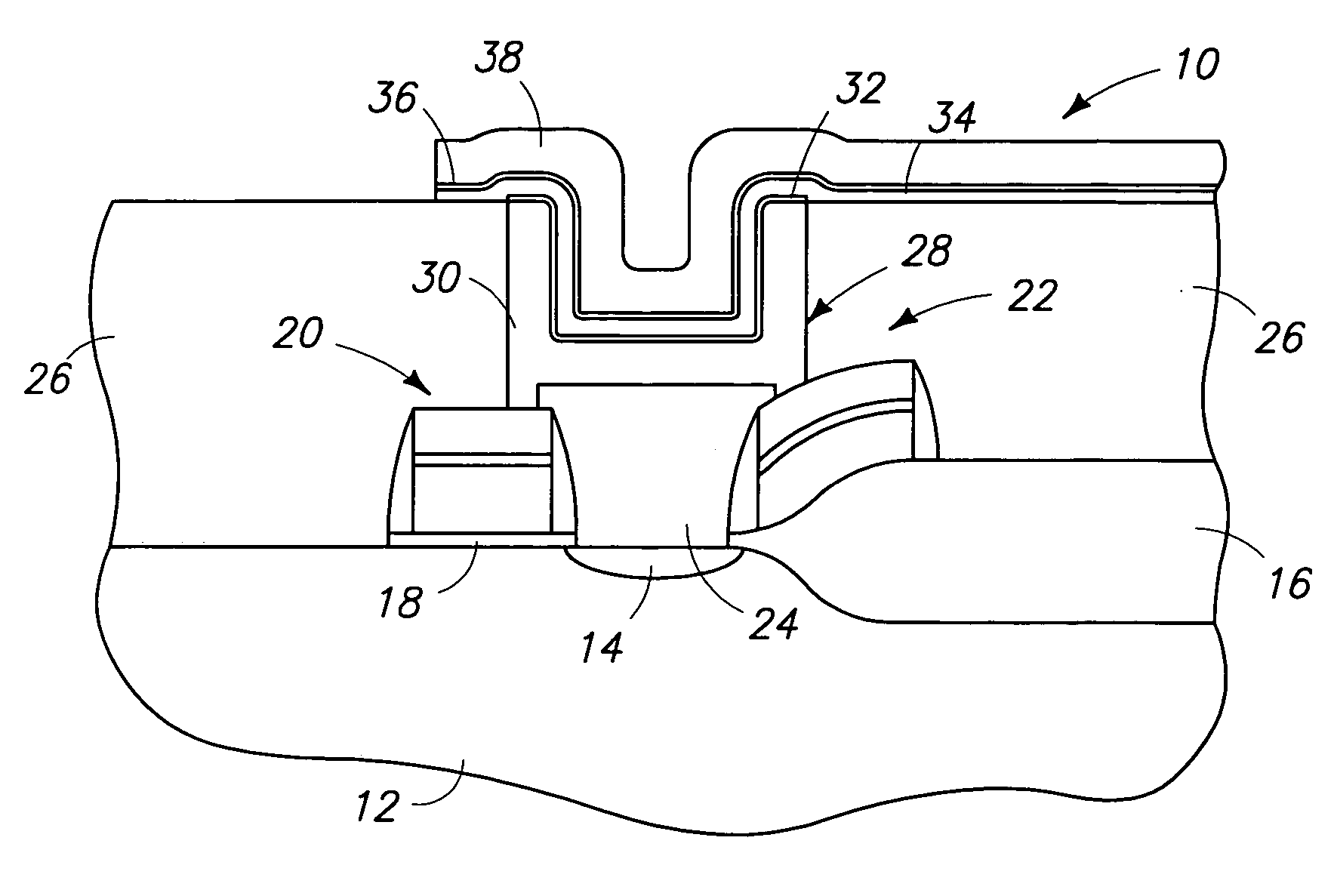
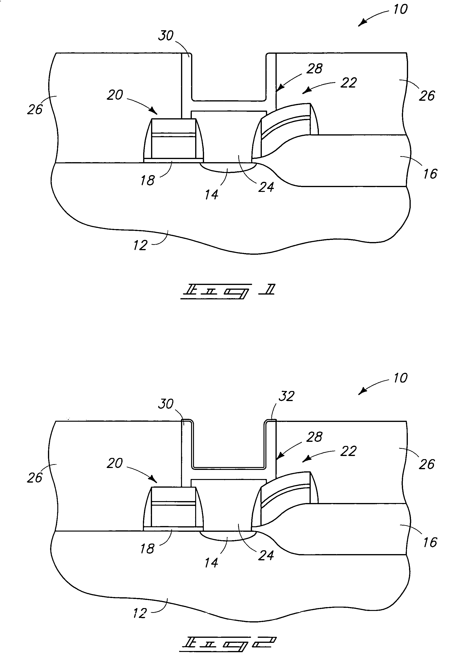
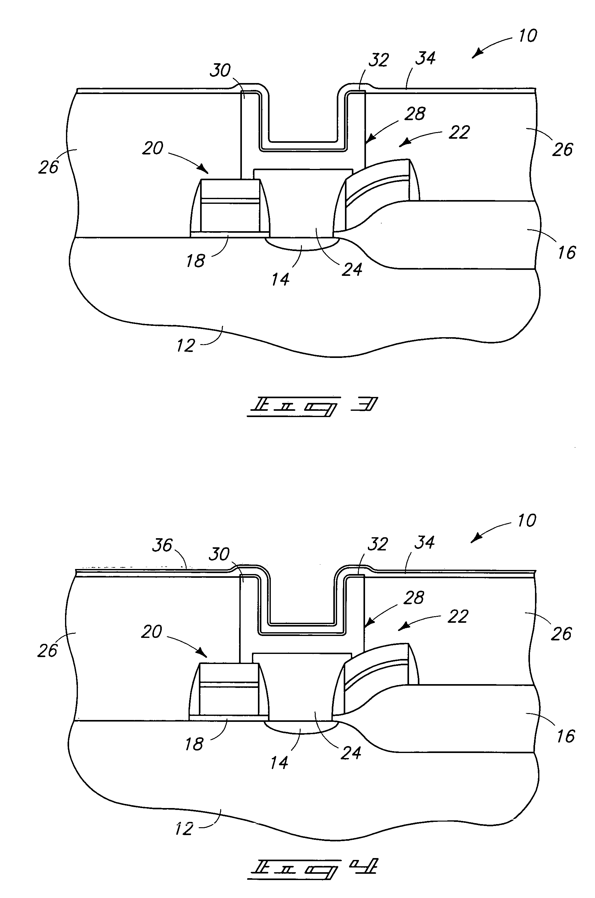
[0020] It has been recognized that the chemical vapor deposition of silicon nitride utilizing silicon hydride gases and ammonia occurs at different rates over the storage node electrode of a DRAM capacitor (including any thin oxide formed thereover) and doped oxides. Specifically, such deposition of silicon nitride is largely selective to the storage node (typically polysilicon), and regardless is at a considerably greater growth rate than what occurs over the BPSG or other doped oxide layers. Accordingly, as the silicon nitride layer thickness over the storage node fell to below 80 Angstroms, an apparent lesser quantity growing over the doped oxide layer resulted in a layer too thin to achieve the barrier layer effect during the subsequent re-oxidation to form the outer oxide layer of ...


PUM

PropertyMeasurementUnit
thicknessaaaaaaaaaa
pressureaaaaaaaaaa
temperatureaaaaaaaaaa

Abstract

A first electrode and a doped oxide layer laterally proximate thereof are provided over a substrate. A silicon nitride layer is formed over both the doped oxide layer and the first electrode to a thickness of no greater than 80 Angstroms over at least the first electrode by low pressure chemical vapor deposition using feed gases comprising a silicon hydride, H2 and ammonia. The substrate with silicon nitride layer is exposed to oxidizing conditions comprising at least 700° C. to form a silicon dioxide layer over the silicon nitride layer, with the thickness of silicon nitride over the doped oxide layer being sufficient to shield oxidizable substrate material beneath the doped oxide layer from oxidizing during the exposing. A second electrode is formed over the silicon dioxide layer and the first electrode. In one implementation, the chemical vapor depositing comprises feed gases of a silicon hydride and ammonia, with the depositing comprising increasing internal reactor temperature from below 500° C. to a maximum deposition temperature above 600° C. and starting feed of the silicon hydride into the reactor at a temperature less than or equal to 600° C. In one implementation the depositing comprises increasing internal reactor temperature from below 500° C. to a maximum deposition temperature above 600° C. using a temperature ramp rate of at least 10° C. / minute from at least 500° C. to at least 600° C. Other aspects and implementations are described.

Description

TECHNICAL FIELD [0001] This invention relates to methods to form electronic devices, for example capacitors, antifuses, transistor gate and other constructions, and to methods to form a material over a semiconductive substrate. BACKGROUND OF THE INVENTION [0002] As the density of DRAM cells increases, there is a continuing challenge to maintain sufficiently high storage capacitance despite decreasing cell area. Additionally, there is a continuing goal to further decrease cell area. One principal way of increasing cell capacitance is through cell structure techniques. Such techniques include three-dimensional cell capacitors, such as trenched or stacked capacitors. Yet as feature sizes continue to become smaller and smaller, development of improved materials for cell dielectrics as well as the cell design and structure become important. The feature size of higher density DRAMS, for example 256 Mb, will be on the order of 0.25 micron and less. Such overall reduction in cell size drive...

Claims


Application Information

Patent Timeline
Patent Type & Authority Applications(United States)
IPC IPC(8): H01L21/8244C23C16/34H01L21/02H01L21/314H01L21/318H01L21/8242
CPCC23C16/345H01L28/40H01L21/02274H01L21/02164H01L21/02129H01L21/02326H01L21/022H01L21/02211H01L21/0217H10B12/033H01L21/3144H01L21/3145H01L21/3185H01L21/02337
Inventor THAKUR, RANDHIR
Owner THAKUR RANDHIR
Why Eureka
Try Eureka