

Driving apparatus and driving method of light emitting display panel
- Summary
- Abstract
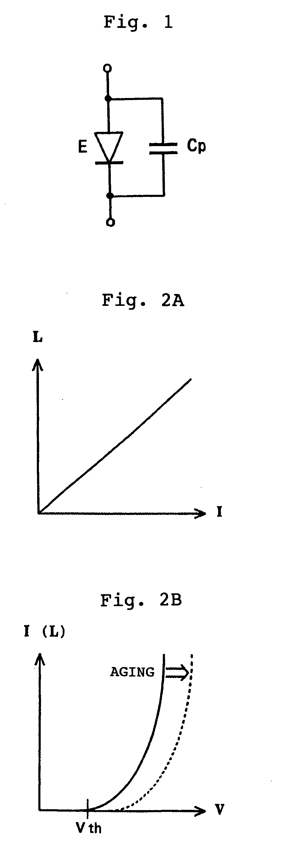
- Description
- Claims
- Application Information
AI Technical Summary
Benefits of technology
Problems solved by technology
Method used
Image

Examples
first embodiment
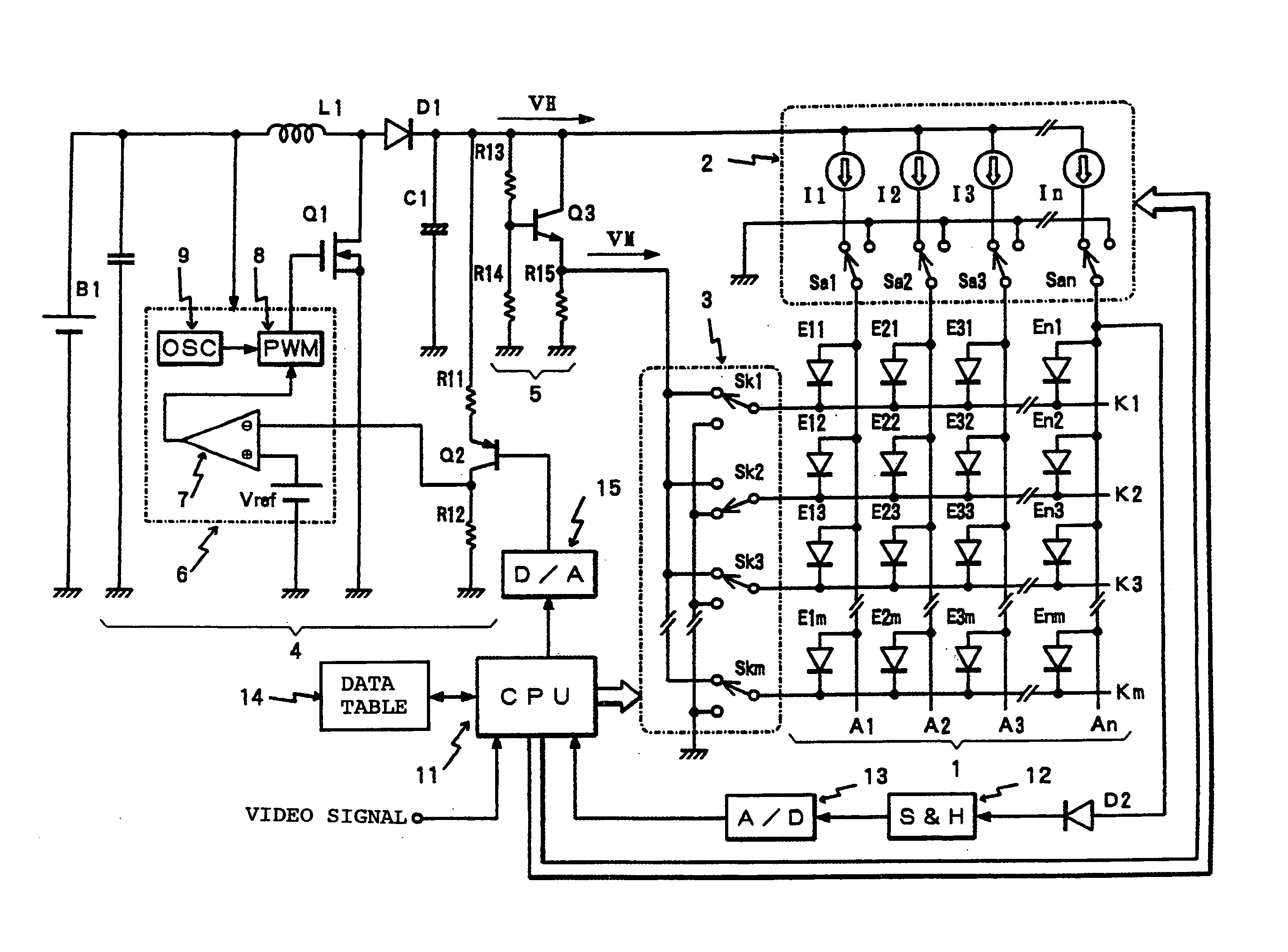
[0040]FIG. 6 is to explain a first embodiment constructed so that the above-described means is utilized to control an output voltage value of the voltage source, and shows an example in which it is adopted in a driving apparatus of a passive drive type display panel.
[0041] The driving method of EL elements in this passive matrix drive system includes two methods, that is, methods of cathode line scan / anode line drive and anode line scan / cathode line drive, and the structure shown in FIG. 6 shows a feature of the former cathode line scan / anode line drive. That is, n anode lines A1-An as supply lines are arranged in a vertical direction (column direction), m cathode lines K1-Km as scan lines are arranged in a horizontal direction (row direction), and organic EL elements E11-Enm represented by symbols of diodes are arranged at portions at which the anode lines intersect the cathode lines (in total, n×m portions) to construct a display panel 1.
[0042] In the respective EL elements E11-E...
second embodiment
[0068]FIG. 8 shows a second embodiment according to the present invention and shows an example in which the present invention is adopted in a driving apparatus of a passive drive type display panel similarly. This FIG. 8 shows parts corresponding to the display panel 1, the anode line drive circuit 2, and the cathode line scan circuit 3 shown in FIG. 6, and since other structures are the same as those shown in FIG. 6, they are omitted in the drawing. Further, in this FIG. 8, parts corresponding to respective parts in FIG. 6 are denoted by the same reference characters, and therefore detailed description thereof will be omitted.
[0069] In the embodiment shown in FIG. 8, other than the constant current sources I1-In which are for driving respective EL elements for lighting, a constant current source Ins as a measurement current supply means which can supply the measurement current Is is provided. The structure shown in FIG. 8 is constructed such that the light emission drive current If...
third embodiment
[0071]FIG. 9 shows a third embodiment according to the present invention and shows an example in which the present invention is adopted in a driving apparatus of an active drive type display panel. In this FIG. 9, parts which achieve functions similar to those of the structure shown in FIG. 6 are denoted by the same reference characters, and as other structures which are not shown in FIG. 9 and which include the DC-DC converter and the like, the structures shown in FIG. 6 can be adopted as they are.
[0072] In FIG. 9, in the light emitting display panel represented by reference numeral 1, display pixels 31 are arranged in a matrix in the vertical and horizontal directions. In FIG. 9, regarding the display pixels 31 arranged in a matrix, for convenience of illustration, two pixels in the respective vertical and horizontal directions, that is, four pixels in total, are shown.
[0073] In the light emitting display panel 1, data lines n1, n2, . . . on which a data signal is supplied from t...
PUM
 Abstract
Description
Claims
Application Information