Method of cutting integrated circuit chips from wafer by ablating with laser and cutting with saw blade

a technology of integrated circuit chips and laser cutting, which is applied in the direction of basic electric elements, electrical equipment, semiconductor devices, etc., can solve the problems of rough top surface of integrated circuit chips, and achieve the effect of different surface textures and different surface textures

Active Publication Date: 2006-08-24
TAIWAN SEMICON MFG CO LTD
View PDF14 Cites 62 Cited by
  • Summary
  • Abstract
  • Description
  • Claims
  • Application Information

AI Technical Summary

Benefits of technology

[0008] In accordance with another aspect of the present invention, a method of forming a packaged integrated circuit chip is provided. This method includes the following steps described in this paragraph. The order of the steps may vary, may be sequential, may overlap, may be in parallel, and combinations thereof. An upper portion of the wafer is ablated using an energy source comprising a laser beam to form a trench that extends into the wafer from a top surface of the wafer through intermetal dielectric layers and at least partially into a substrate of the wafer. The wafer has a plurality of integrated circuit chips. The trench is formed between at least two of the chips of the wafer. After the ablating to form the trench, cutting through the wafer between outer sidewalls of the laser-ablated trench with a saw blade is performed. A width between the outer sidewalls of the two laser-ablated trenches is greater than a cutting width of the saw blade. An integrated circuit chip is cut, wherein the cutting includes the ablating and saw cutting steps. The cut integrated circuit chip is attached and electrically connected to a package substrate using solder bumps. The solder bumps may be substantially lead-free, or alternatively, the solder bumps may include lead. The intermetal dielectric layers may include at least one layer of low-k dielectric material. The method of the above embodiment may also include a second trench substantially parallel to the laser-ablated trench. The second trench may be formed by a second laser beam in-situ or after the laser beam mentioned above and followed by the saw blade cutting.
[0009] In accordance with yet another aspect of the present invention, an integrated circuit chip is provided, which includes a low-k dielectric layer, a chip substrate, and an edge of the integrated circuit chip. The edge of the integrated circuit chip includes a first edge portion and a second edge portion. At least part of the first edge portion being across a same level as the low-k dielectric layer. The first edge portion has been laser ablated to have a series of rounded recesses formed therein. The second edge portion is across a same level as at least part of the chip substrate. The second edge portion has a sawed edge pattern, and the second edge

Problems solved by technology

A top surface of the integrat

Method used


Image

  • Method of cutting integrated circuit chips from wafer by ablating with laser and cutting with saw blade
  • Method of cutting integrated circuit chips from wafer by ablating with laser and cutting with saw blade
  • Method of cutting integrated circuit chips from wafer by ablating with laser and cutting with saw blade

Examples


Embodiment Construction

[0022] Referring now to the drawings, wherein like reference numbers are used herein to designate like or similar elements throughout the various views, illustrative embodiments of the present invention are shown and described. The figures are not necessarily drawn to scale, and in some instances the drawings have been exaggerated and / or simplified in places for illustrative purposes only. One of ordinary skill in the art will appreciate the many possible applications and variations of the present invention based on the following illustrative embodiments of the present invention.

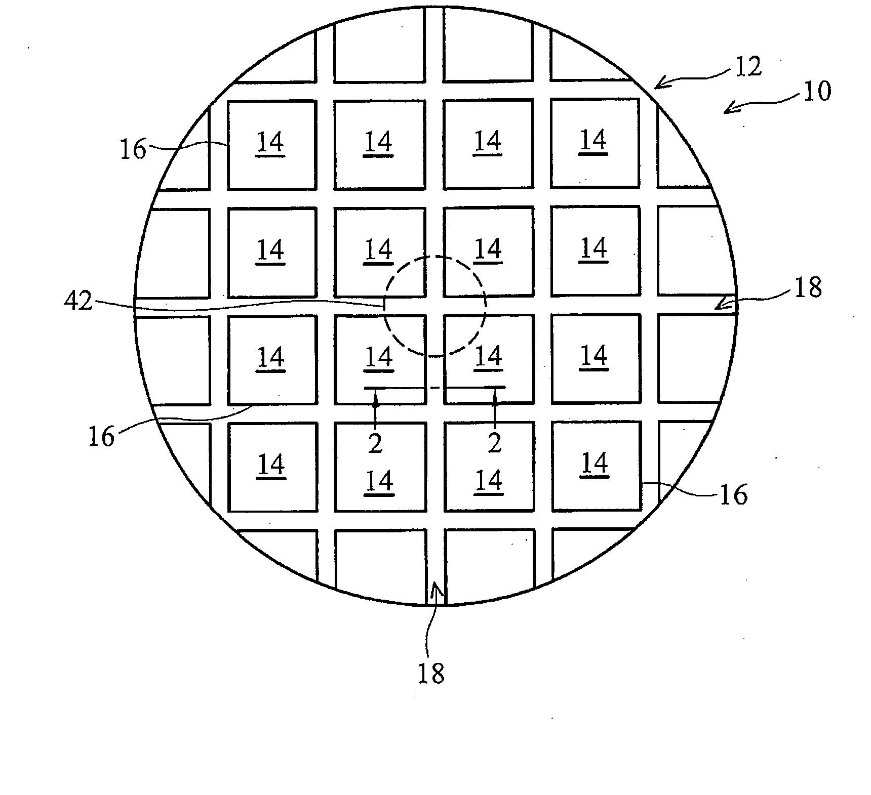
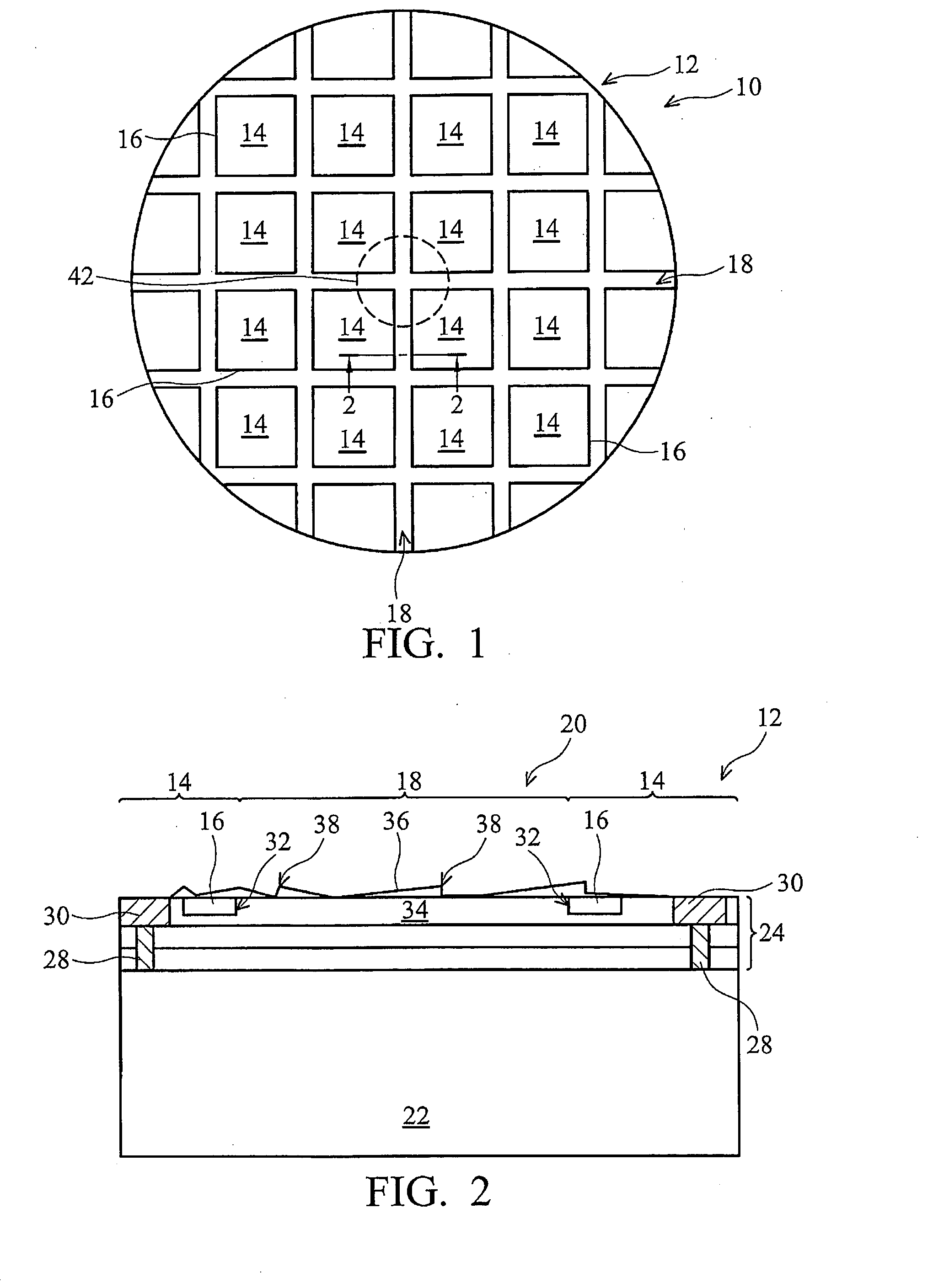
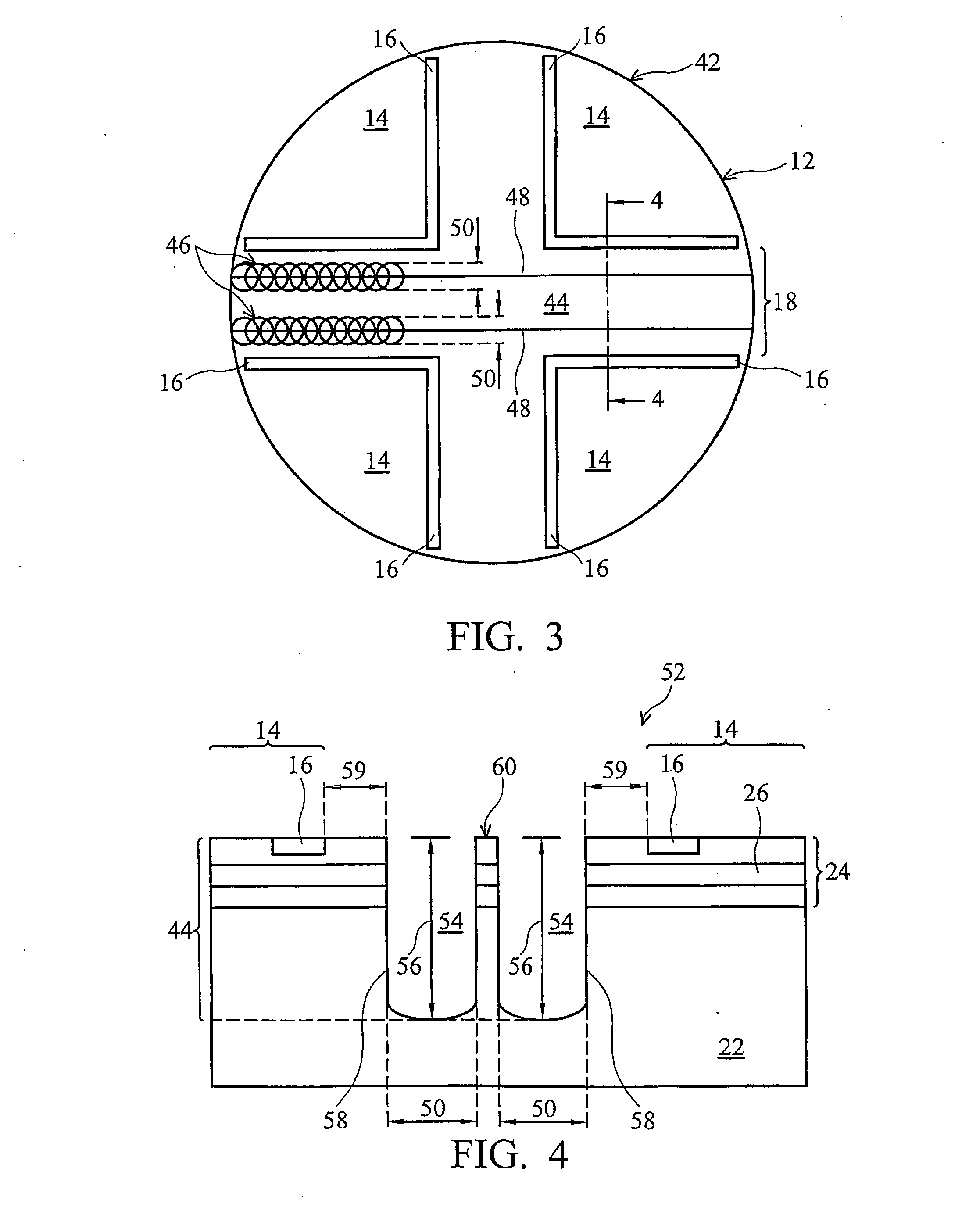
[0023] Generally, an embodiment of the present invention provides a method of cutting integrated circuit chips from a wafer by ablating the wafer with two lasers, forming two parallel trenches along the cutting streets, and then cutting the wafer with a saw blade. FIG. 1 is an overhead view 10 of a wafer 12 in accordance with the first illustrative embodiment of the present invention. Integrated circuit (IC...


PUM


Abstract

A method of cutting an integrated circuit chip from a wafer having a plurality of integrated circuit chips is provided. An upper portion of the wafer is ablated using two laser beams to form two substantially parallel trenches that extend into the wafer from a top surface of the wafer through intermetal dielectric layers and at least partially into a substrate of the wafer. After the ablating to form the two trenches, cutting through the wafer between outer sidewalls of the two laser-ablated trenches with a saw blade is performed. A width between the outer sidewalls of the two laser-ablated trenches is greater than a cutting width of the saw blade. This may be particularly useful in lead-free packaging applications and/or applications where the intermetal dielectric layers use low-k dielectric materials, for example.

Description

[0001] This application claims the benefit of U.S. Provisional Application No. 60 / 654,285 filed on Feb. 18, 2005 entitled Method Of Singulating Integrated Circuit Chips From Wafer By Ablating With Laser And Cutting With Saw Blade, which application is hereby incorporated herein by reference.TECHNICAL FIELD [0002] The present invention generally relates to manufacturing and packaging integrated circuit chips. In one aspect, it relates more particularly to cutting integrated circuit chips from a wafer by ablating with laser beams and cutting with a saw blade. BACKGROUND [0003] To reduce signal delay and improve electrical performance in high speed integrated circuits, low-k dielectric materials (having a dielectric constant less than 3.9) are often implemented for the intermetal dielectric (IMD) layers of an integrated circuit chip. Low-k and ultra low-k dielectric materials are currently preferred for use in the IMD layers to reduce RC delay and parasitic capacitances. The general tr...

Claims


Application Information

Patent Timeline
IPC IPC(8): H01L21/78
CPCH01L21/78H01L2224/13116H01L2224/16225H01L2224/32225H01L2224/73204H01L2924/00H01L2224/0557H01L2224/05573H01L2224/056H01L2224/05571H01L2924/00014H01L2224/0554H01L2224/05599H01L2224/0555H01L2224/0556
Inventor LU, SZU WEILEE, HSIN-HUISUNG, MING-CHUNGLII, MIRNG-JI
Owner TAIWAN SEMICON MFG CO LTD
Why Eureka
Try Eureka