Optical signal reception device

a technology of optical signals and reception devices, applied in the field of optical signal reception devices, can solve problems such as the degraded waveform of optical signals, and achieve the effect of quick identification of signal reception states and frame synchronization

Inactive Publication Date: 2006-08-31
FUJITSU LTD
View PDF0 Cites 38 Cited by
  • Summary
  • Abstract
  • Description
  • Claims
  • Application Information

AI Technical Summary

Benefits of technology

[0057] According to the present invention, when the reception frame processing unit detects-out-of-frame-synchronization (LOF (Loss of Frame) or OOF (Out of Frame)), the controller controls logical inversion operations in the clock regenerator, a multiplexing timing in the multiplexer, and controls the delay interferometer in the front end; thereby, it is possible to perform frame synchronization pull-in operations to attain an object signal reception state.
[0058] In addition, by providing a frame synchronization circuit in the reception frame processing unit that includes plural frame synchronization units corresponding to combinations of plural synchronization bit strings, it is possible to quickly identify the signal reception state, and it is possible to perform the frame synchronization pull-in operations quickly to attain the object signal reception state.
[0060] According to the present invention, because the front end includes a polarization controller, a delay interferometer, a polarizing beam splitter, and a differential light receiver, the signal reception device includes only one delay interferometer; hence it is possible to make the signal reception device compact and simplify control of the signal reception device.

Problems solved by technology

However, when DQPSK optical signals are transmitted through an optical transmission path, waveforms of the optical signals may be degraded because of influences of wavelength dispersion and the non-linear effect of the optical fiber in use.

Method used


Image

  • Optical signal reception device
  • Optical signal reception device
  • Optical signal reception device

Examples


first embodiment

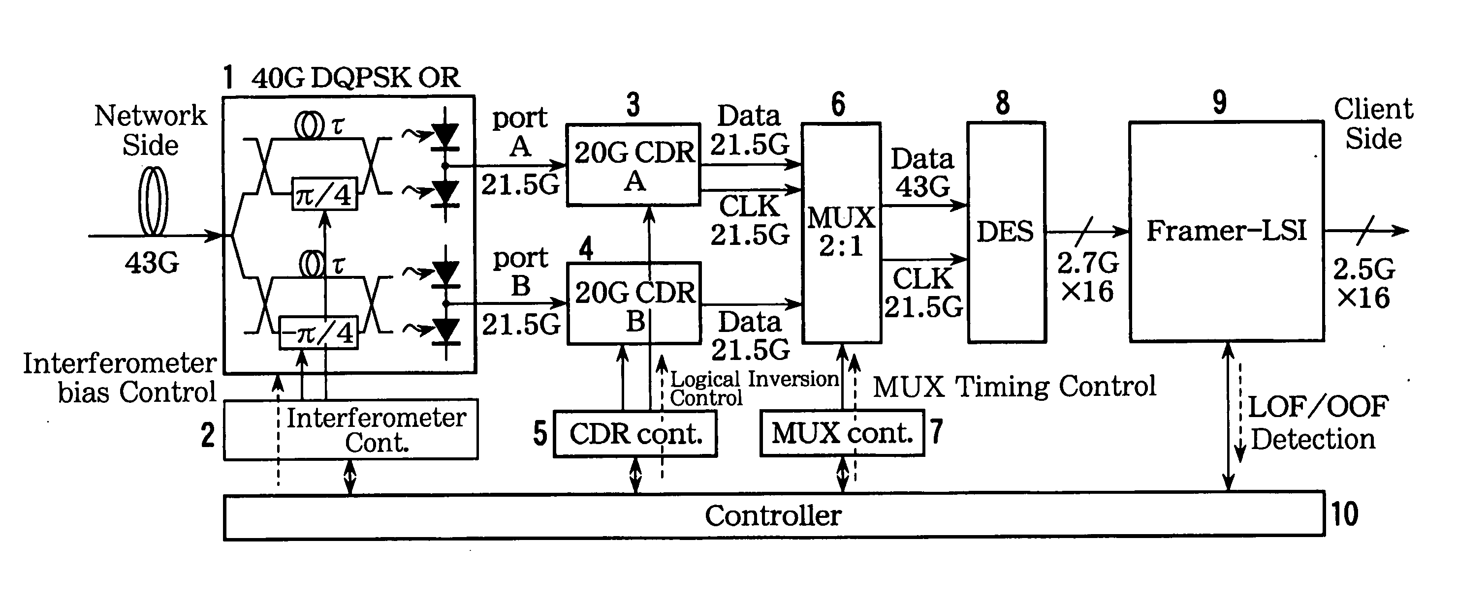
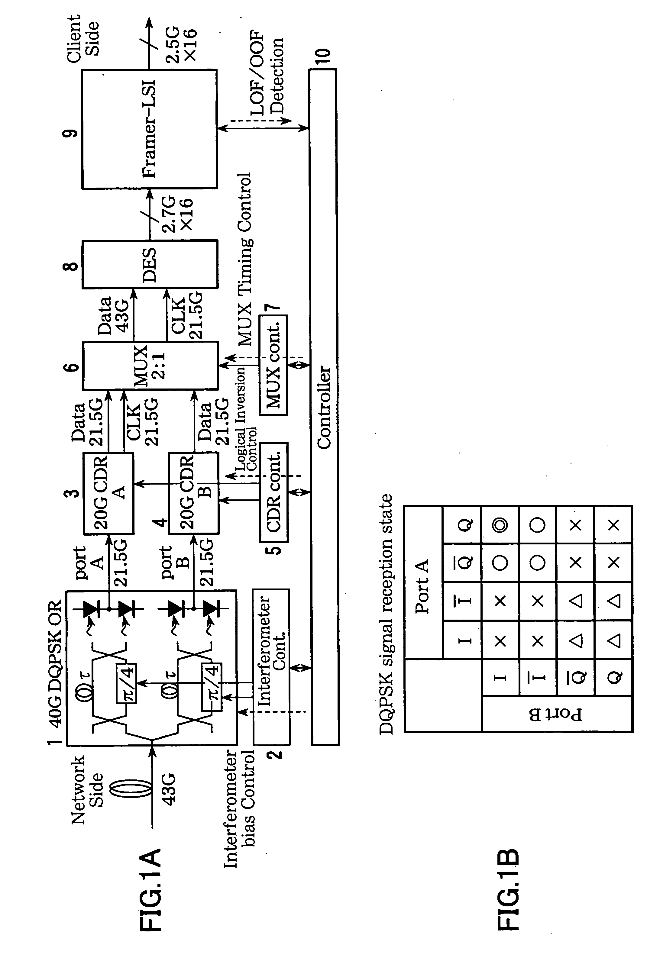
[0102]FIG. 1A is a block diagram illustrating a principal portion of an optical signal receiver according to a first embodiment of the present invention, used in an optical communication system for transmitting the DQPSK optical signals.

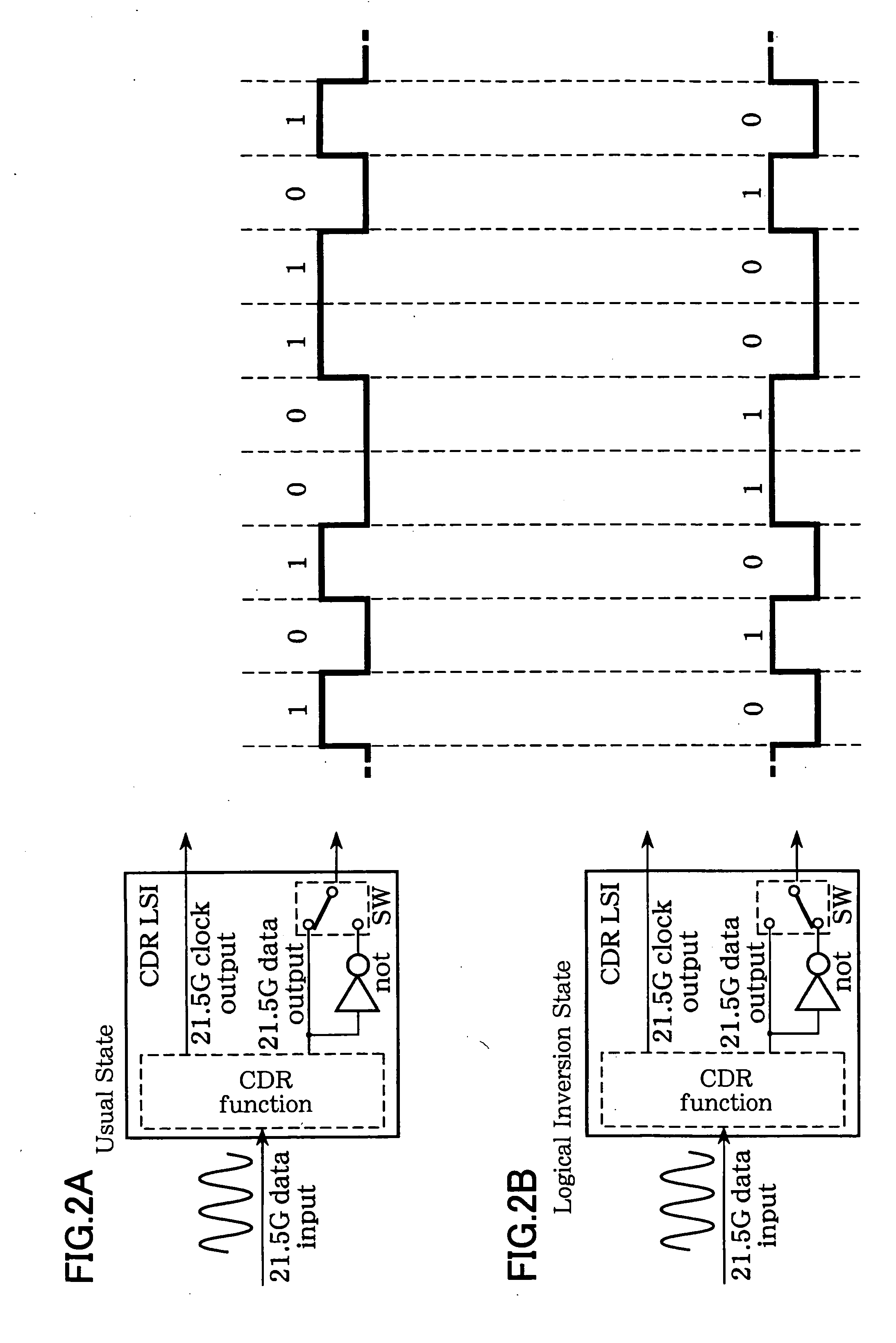
[0103] The optical signal receiver illustrated in FIG. 1A includes a front end 1 that has two delay interferometers and opto-electric conversion elements that receives DQPSK optical signals and converts the DQPSK optical signals into in-phase signals I and orthogonal signals Q; clock regenerators 3 and 4 that regenerate clock signals CLK based on the in-phase signals I and the orthogonal signals Q; a multiplexer 6 that multiplexes the in-phase signals I and the orthogonal signals Q output from the clock regenerators 3 and 4; a reception frame processing unit 9 that detects frame synchronization based on the signals multiplexed by the multiplexer 6; and a controller 10 that, based on an out-of-frame-synchronization detection result (LOF (Loss of Fram...

second embodiment

[0123]FIG. 4 is a block diagram illustrating a principal portion of an optical signal receiver according to a second embodiment of the present invention; specifically, FIG. 4 illustrates a principal portion of the reception frame processing unit 9 (framer LSI) as shown in FIG. 1A.

[0124] As illustrated in FIG. 4, the reception frame processing unit 9 includes a frame processor 21, a frame synchronization circuit 22, and a signal reception state identifier 23 for identifying signal reception states of DQPSK signals.

[0125] In addition, 16 parallel signals each at 2.7 Gbps are input to the reception frame processing unit 9.

[0126] The frame synchronization circuit 22 includes 16 frame synchronizers FSC01 through FSC16, which perform frame synchronization detection on different combinations of synchronization bit strings. In an OTN (Optical Transport Network) signal, as recommended by ITU-T G.709, it is known that a header of a frame is identified by detecting a Frame Alignment Signal ...

third embodiment

[0137]FIG. 6 is a block diagram illustrating a principal portion of an optical signal receiver according to a third embodiment of the present invention; specifically, FIG. 6 illustrates a principal portion of the reception frame processing unit 9 (framer LSI) as shown in FIG. 1A.

[0138] As illustrated in FIG. 6, the reception frame processing unit 9 includes a frame processor 21a, a frame synchronization circuit 22a, an OTUk-FAS detection circuit 25, and registers 26. The same as FIG. 4, 16 parallel signals each at 2.7 Gbps from the de-serializer (DES) 8 are input to the reception frame processing unit 9.

[0139] The frame synchronization circuit 22a detects predetermined synchronization bits to detect frame synchronization, and sends a frame synchronization signal to the frame processor 21.

[0140] In OTN (Optical Transport Network) systems, as recommended by ITU-T G.709, Frame Alignment Signal (FAS) bytes are defined as the frame synchronization bits in an overhead section of an OTU...


PUM


Abstract

An optical signal reception device is disclosed that receives and demodulates an optical signal modulated by DQPSK and performs logical inversion and other controls to transit to the object reception state. The signal reception device includes a front end including a delay interferometer and an opto-electric conversion element that receive the DQPSK optical signal and convert it into an in-phase signal and an orthogonal signal, a clock regenerator that regenerates a clock signal based on the in-phase signal and the orthogonal signal, a multiplexer that multiplexes the in-phase signal and the orthogonal signal, a reception frame processing unit that detects frame synchronization based on the signal multiplexed by the multiplexer and de-maps the received frames, and a controller that, based on out-of-frame-synchronization information (LOF / OOF) from the reception frame processing unit, performs logical inversion control in the clock regenerator, multiplexing timing control in the multiplexer, and controls the delay interferometer in the front end so as to transit to the object reception state.

Description

BACKGROUND OF THE INVENTION [0001] 1. Field of the Invention [0002] The present invention relates to an optical signal reception device for receiving and demodulating optical signals modulated by a Differential Quadrature Phase Shift Keying (DQPSK) modulation scheme or a Differential Phase Shift Keying (DPSK) modulation scheme in order to achieve high speed data transmission. [0003] 2. Description of the Related Art [0004] In digital communication systems, typically the Internet (IP: Internet Protocol), in order to meet rapidly increasing needs of digital communication, an optical communication scheme employing IM-DQPSK (Intensity Modulation Differential Quadrature Phase Shift Keying) modulation scheme is being studied to improve utilization of frequencies. [0005] For details of IM-DQPSK, reference can be made to P. S. Cho, V. S. Grigoryan, Y. A. Godin, A. Salamon, and Y. Achiam, “Transmission of 25 Gbps RZ-DQPSK signals with 25-GHz channel spacing over 1000 km of SMF-28 fiber”, IEE...

Claims


Application Information

Patent Timeline
Patent Type & Authority Applications(United States)
IPC IPC(8): H04B10/04H04B10/07H04B10/40H04B10/25H04B10/50H04B10/516H04B10/524H04B10/548H04B10/58H04B10/60H04B10/61H04B10/67H04B10/69H04L27/22
CPCH04B10/66H04L27/223
Inventor KATAGIRI, TORUHOSHIDA, TAKESHITAKAHARA, TOMOONAKAMURA, KENTAROKUWATA, NAOKI
Owner FUJITSU LTD
Why Eureka
Try Eureka