
Magnetic memory device and write method of magnetic memory device

a magnetic memory device and write method technology, applied in the magnetic memory device field, can solve the problems of increasing the reversal field of the recording layer of the mtj element, the inability to increase the capacity of the memory device, and the inherently small write margin, etc., to achieve the effect of small reversal field, small reversal field, and large memory energy

Inactive Publication Date: 2006-09-07
KK TOSHIBA
View PDF3 Cites 3 Cited by
  • Summary
  • Abstract
  • Description
  • Claims
  • Application Information

AI Technical Summary

Problems solved by technology

For conventional magnetic random access memories, however, it is becoming clear that the capacity can hardly be increased because the write current value increases as the circuit is micropatterned, and the write margin which is small inherently further decreases as the circuit is micropatterned.
This results in an increase in reversal field of the recording layer of the MTJ element.
As described above, the most important challenges in the conventional magnetic random access memories are to maintain nonvolatility, reduce the reversal field of the recording layer of the MTJ element, and reduce the write current value to achieve high integration.

Method used


Image

  • Magnetic memory device and write method of magnetic memory device
  • Magnetic memory device and write method of magnetic memory device
  • Magnetic memory device and write method of magnetic memory device

Examples


first angle example

(First Angle Example)

[0083] In the first angle example, 0°≦θ≧30° is set to further reduce the write current value.

[0084]FIGS. 8A and 8B are views for explaining the effect of the first angle example of oblique arrangement of the MTJ element according to the embodiment of the present invention.

[0085] As shown in FIG. 8A, in the first angle example, the angle 0 made by the direction of axis of easy magnetization of the MTJ element 10 and the running direction (X-axis direction) of the first write wiring W1 falls within the range of 0° (exclusive) to 30° (inclusive) (θ30°, the write driver considerably becomes large, and the cost increases.

[0086] In this case, as shown in FIG. 8B, the write current value (Hswx′ or Hswy′ on the magnetic field basis) of the write wiring turned on first can be halved. In addition, the write current value (Hswy′ or Hswx′ on the magnetic field basis) of the other write wiring turned on next can also be halved. For example, when θ≦30°, the practical write...

second angle example

(Second Angle Example)

[0087] In the second angle example, 5°≦θ≦30° is set to optimize the write margin for a variation in asteroid curve.

[0088]FIGS. 9A and 9B are views for explaining the effect of the second angle example of oblique arrangement of the MTJ element according to the embodiment of the present invention.

[0089] As shown in FIG. 9A, in the second angle example, the angle θ made by the direction of axis of easy magnetization of the MTJ element 10 and the running direction (X-axis direction) of the first write wiring W1 falls within the range of 5° (inclusive) to 30° (inclusive) (5°≦θ≦30°). The reason why θ≧5° is that if θ<5°, anti-parallel magnetization reversal was sometimes observed in the semi-selected state (semi-selected state in which only Hx is applied in FIG. 9A).

[0090] In this case, as shown in FIG. 9B, the structure can cope with a typical variation of about 3% in asteroid curve, and the write margin can be ensured. On the magnetic field basis, the reversal fi...

third angle example

(Third Angle Example)

[0091] In the third angle example, θ≦10° is set to implement an ideal asteroid curve. When θ≦10°, the write current value can be made as small as about 3 mA, and the asteroid curve can be located almost at the center of the upper-right quadrant.

[0092]FIGS. 10A and 10B are views for explaining the third angle example of oblique arrangement of the MTJ element according to the embodiment of the present invention. FIG. 11 shows the relationship between the angle and the applied field in the write operation in the third angle example shown in FIGS. 10A and 10B.

[0093] As shown in FIG. 10A, in the third angle example, the angle θ made by the direction of axis of easy magnetization of the MTJ element 10 and the running direction (X-axis direction) of the first write wiring W1 is 10° or less (θ≦10°). The lower limit value of the angle θ in the third angle example can be either 0<θ or 5≧θ.

[0094] The write operation in the third example will be described below. The effe...


PUM


Abstract

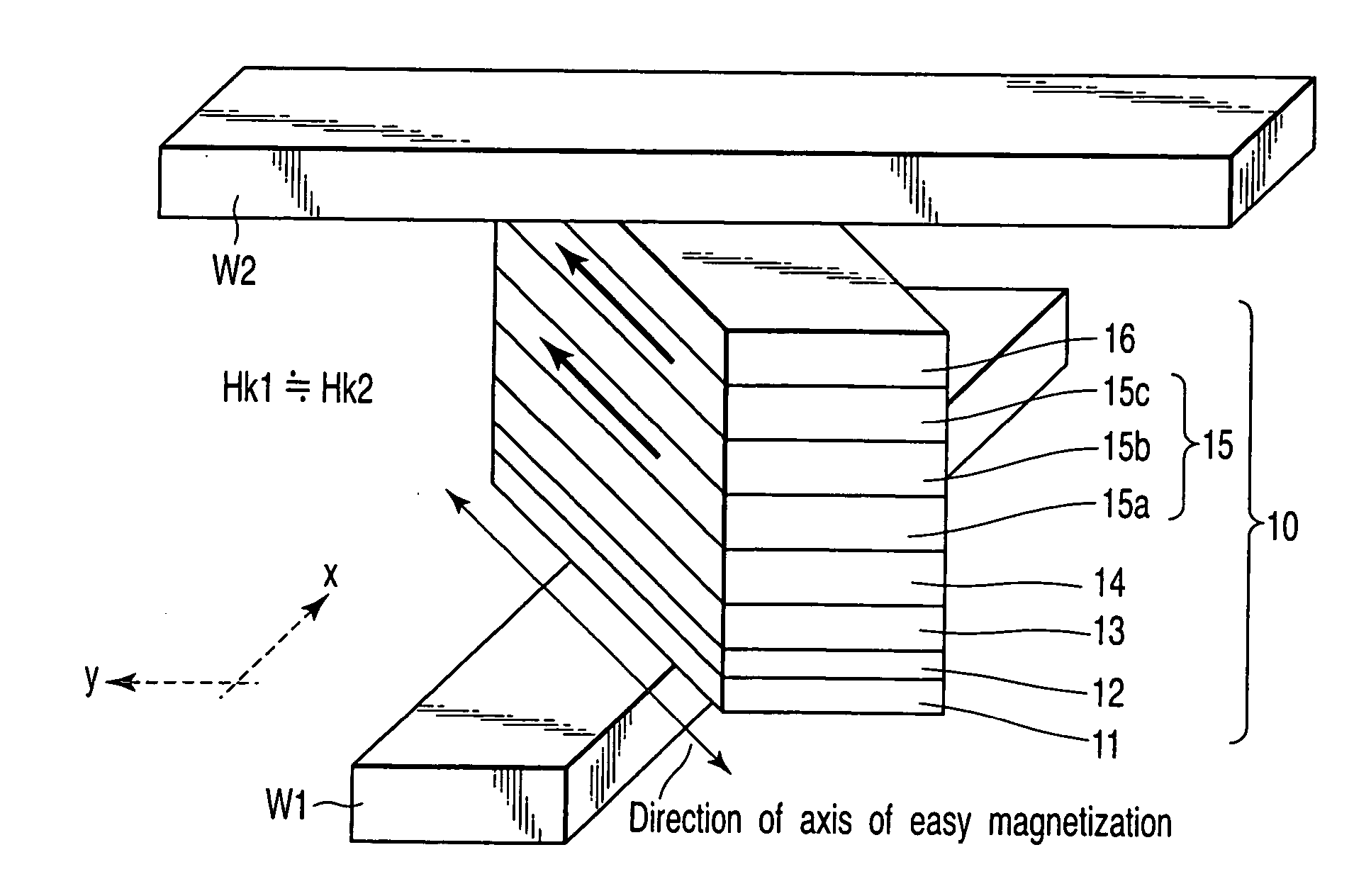
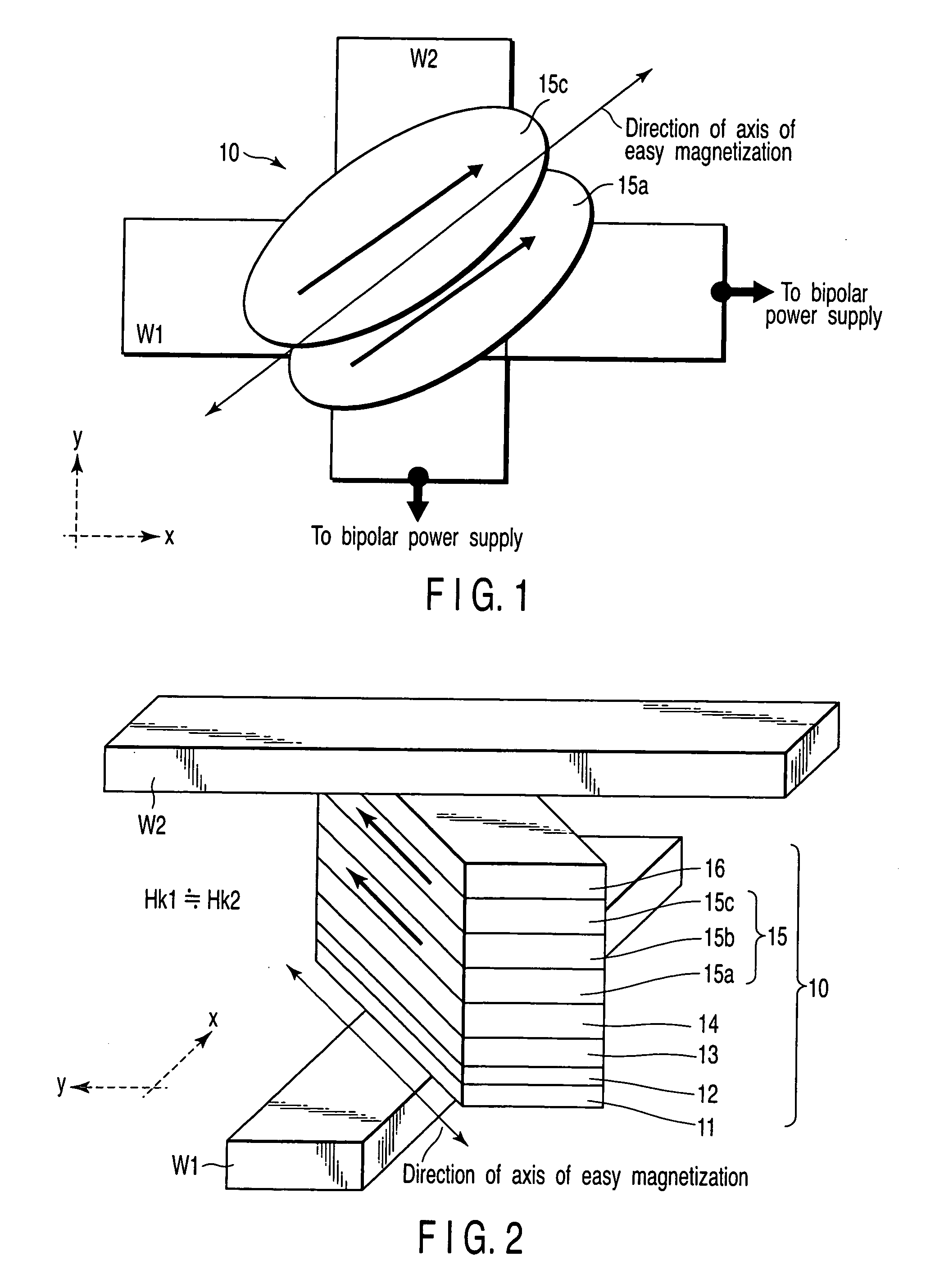
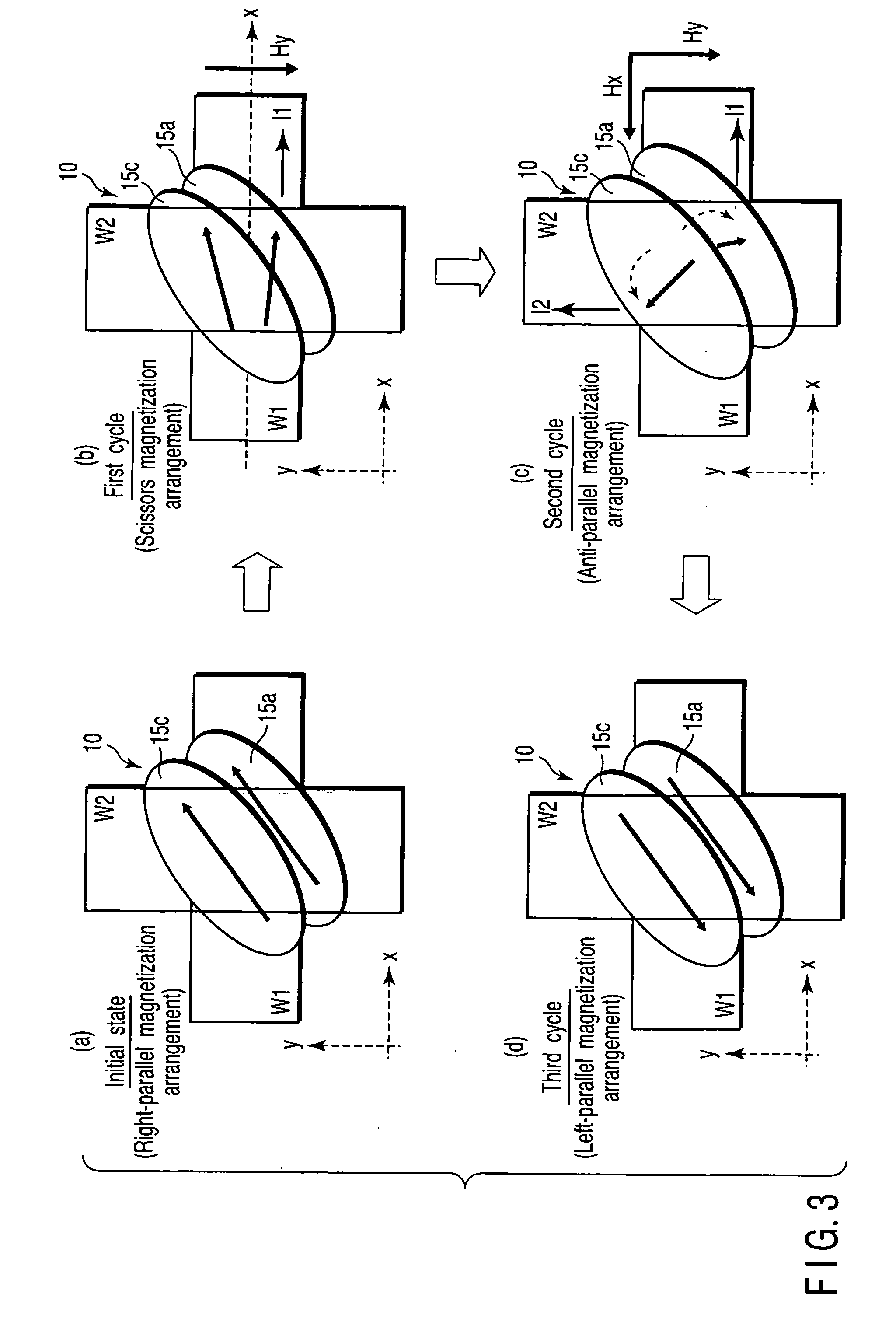
A magnetic memory device includes a first write wiring which runs in a first direction, a second write wiring which runs in a second direction different from the first direction, and a magnetoresistive element which is arranged at an intersection between the first and second write wirings, has a fixed layer, a recording layer, and a magnetoresistive layer sandwiched between the fixed layer and the recording layer, and has an axis of easy magnetization obliquely with respect to the first and second directions, the recording layer including a first ferromagnetic layer, a second ferromagnetic layer, and a first nonmagnetic layer sandwiched between the first and second ferromagnetic layers, in which first magnetization of the first ferromagnetic layer and second magnetization of the second ferromagnetic layer are ferromagnetically coupled, and a ferro-coupling constant C of a ferromagnetic coupling is 0.0001 erg / cm2≦C≦0.2 erg / cm2.

Description

CROSS-REFERENCE TO RELATED APPLICATIONS [0001] This application is based upon and claims the benefit of priority from prior Japanese Patent Application No. 2005-050625, filed Feb. 25, 2005, the entire contents of which are incorporated herein by reference. BACKGROUND OF THE INVENTION [0002] 1. Field of the Invention [0003] The present invention relates to a magnetic memory device and a write method of the magnetic memory device and, more particularly, to a magnetic random access memory (MRAM) and a write method of it. [0004] 2. Description of the Related Art [0005] Magnetic random access memories (MRAMs) are expected as ultimate memories with nonvolatility, high speed, large capacity, and low voltage driving and developed. [0006] For conventional magnetic random access memories, however, it is becoming clear that the capacity can hardly be increased because the write current value increases as the circuit is micropatterned, and the write margin which is small inherently further decr...

Claims


Application Information

Patent Timeline
Patent Type & Authority Applications(United States)
IPC IPC(8): G11C11/14
CPCG11C11/16
Inventor YODA, HIROAKIKAI, TADASHINAKAYAMA, MASAHIKOIKEGAWA, SUMIOKISHI, TATSUYA
Owner KK TOSHIBA
Learn More