Electro-optical device, method of manufacturing electro-optical device, and electronic apparatus

Inactive Publication Date: 2006-09-14
EPSON IMAGING DEVICES CORP
View PDF5 Cites 9 Cited by
  • Summary
  • Abstract
  • Description
  • Claims
  • Application Information

AI Technical Summary

Benefits of technology

[0007] An advantage of some aspects of the invention is that it provides an electro-optical device having a driving circuit and capable of being manufactured by a simple process with high yield, and a method of manufacturing the same.

Problems solved by technology

When the driving circuit is formed on an element substrate by using a semiconductor film, the driving capability of a driving circuit using an amorphous semiconductor film is insufficient.
However, the former is effective to narrow a frame, but has a problem in that the process becomes complicated because the pixel part and the driving circuit are formed at the same time, resulting in low yield.
Furthermore, the driving circuit formed by using the low-temperature polysilicon process has lower static electricity resistance than IC chips, and thus it is required to carefully handle the driving circuit.
In this case, when the first connecting part and the second connecting part are formed on the inside of the sealing material, there is a possibility that a conductive member for connecting the connecting parts will come into contact with the electro-optical material, resulting in the deterioration of the electro-optical material.

Method used


Image

  • Electro-optical device, method of manufacturing electro-optical device, and electronic apparatus
  • Electro-optical device, method of manufacturing electro-optical device, and electronic apparatus
  • Electro-optical device, method of manufacturing electro-optical device, and electronic apparatus

Examples


Embodiment Construction

Liquid Crystal Device

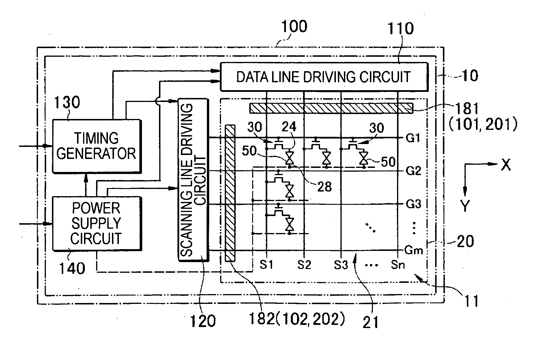
[0040] Preferred embodiments of the invention will be described with reference to the accompanying drawings. This embodiment relates to an active matrix liquid crystal device using TFTs to which an electro-optical device according to the invention is applied.

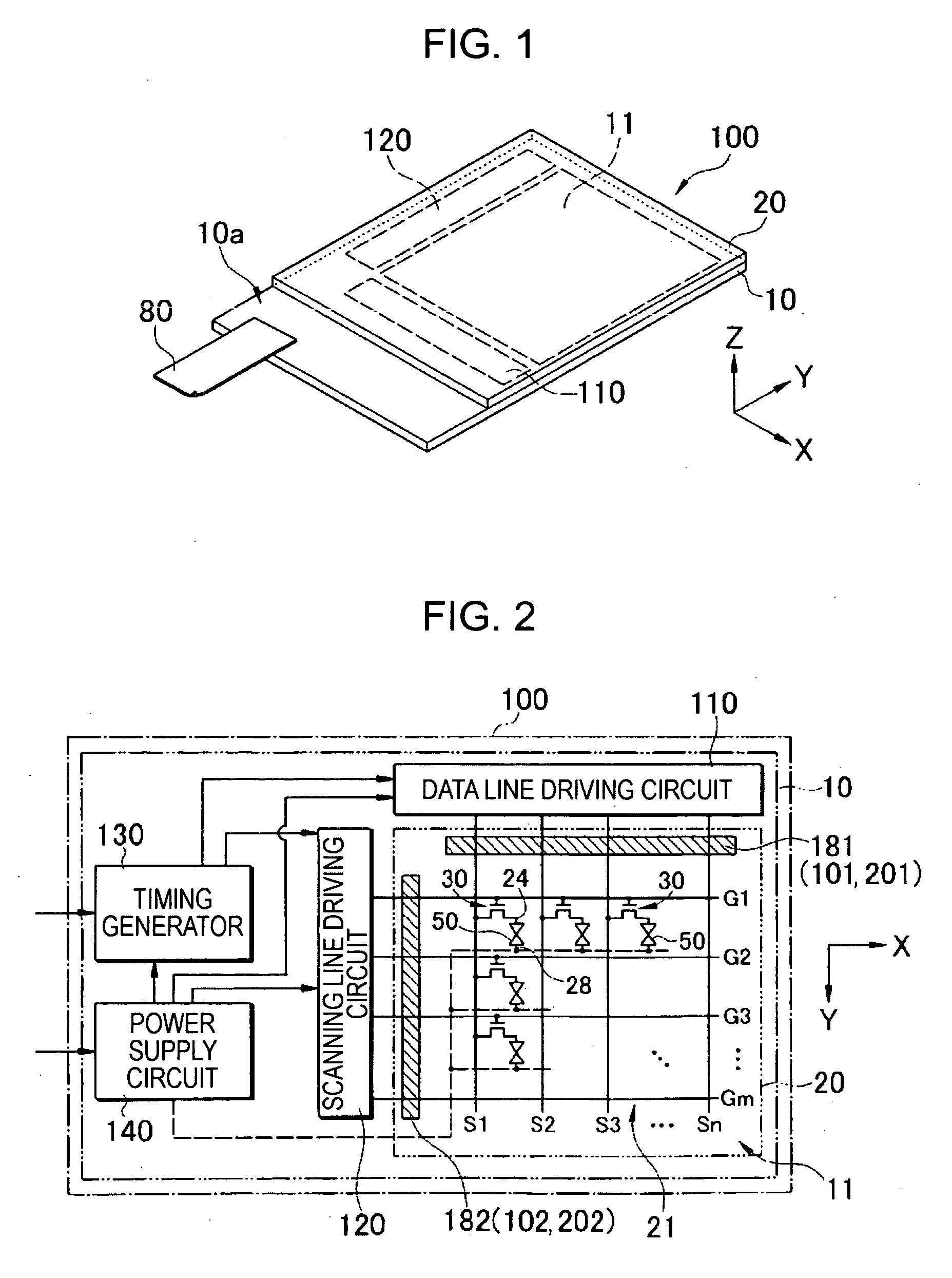
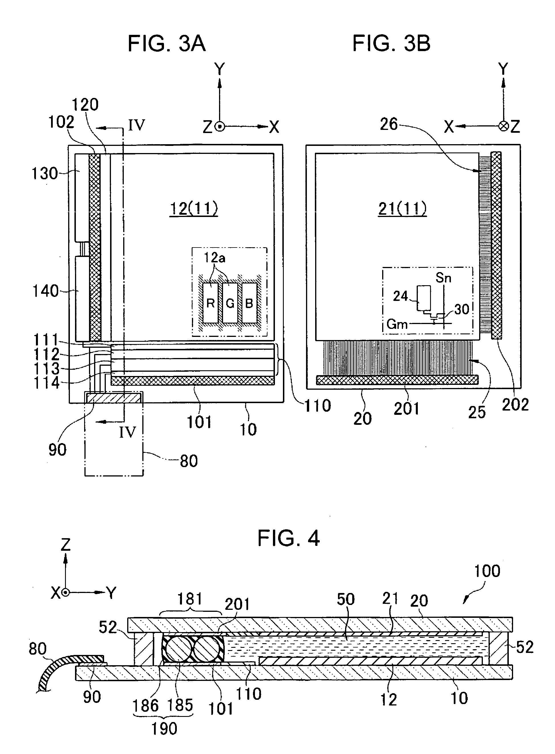
[0041]FIG. 1 is a perspective view showing the configuration of the liquid crystal device according to this embodiment. FIG. 2 is a circuit diagram of the liquid crystal device. FIG. 3A is a plan view showing the configuration of one of two substrates constituting the liquid crystal device, and FIG. 3B is a plan view showing the configuration of the other of two substrates constituting the liquid crystal device. FIG. 4 is a cross-sectional view taken along the line IV-IV of FIG. 3A. FIG. 5 is an explanatory view partially showing the plane-view structure of a connection region 181 shown in FIG. 4.

[0042] As shown in FIG. 1, a liquid crystal device 100 has a driving circuit substrate (first substrate) 10 a...


PUM


Abstract

An electro-optical device includes a first substrate and a second substrate disposed so as to be opposite to each other; a driving circuit part that has a polycrystalline semiconductor layer and is provided on a surface of the first substrate opposite to the second substrate; a first connecting part that is provided on the surface of the first substrate opposite to the second substrate so as to be electrically connected to the driving circuit part; pixel electrodes that are provided on a surface of the second substrate opposite to the first substrate; and a second connecting part that is provided on the surface of the second substrate opposite to the first substrate so as to be electrically connected to the pixel electrodes. The first connecting part and the second connecting part are electrically connected to each other in a region where the first connecting part and the second connecting part overlap each other in plan view.

Description

BACKGROUND [0001] 1. Technical Field [0002] The present invention relates to an electro-optical device, to a method of manufacturing the same, and to an electronic apparatus. [0003] 2. Related Art [0004] In general, a technique of forming a pixel part having pixel switching elements, such as thin film transistors (hereinafter, referred to as TFTs), and a driving circuit for supplying driving signals to the pixel part on the same substrate has been known as a technique for narrowing a frame of an active matrix electro-optical device and for reducing the power consumption of the device. When the driving circuit is formed on an element substrate by using a semiconductor film, the driving capability of a driving circuit using an amorphous semiconductor film is insufficient. Therefore, it has been attempted to form both the pixel switching elements and the driving circuit by using polysilicon semiconductor layers. [0005] For example, JP-A-2002-258765 discloses an electro-optical device i...

Claims


Application Information

Patent Timeline
IPC IPC(8): G09G3/36
CPCG02F1/133351G02F1/1362G02F1/136227
Inventor KOIDE, SHIN
Owner EPSON IMAGING DEVICES CORP
Why Eureka
Try Eureka