Semiconductor integrated device

a technology of integrated circuits and semiconductors, applied in the direction of information storage, static storage, digital storage, etc., can solve the problems of difficult discrimination between storage information between 0 and 1 and achieve the effect of high reliability, high reliability, and high functionality of personal computers

Active Publication Date: 2006-09-14
RENESAS ELECTRONICS CORP
View PDF13 Cites 67 Cited by
  • Summary
  • Abstract
  • Description
  • Claims
  • Application Information

AI Technical Summary

Benefits of technology

[0021] A highly reliable semiconductor non-volatile memory device is implemented for multiple write operations with the semiconductor integrated circuit device of the present invention. This device is also capable to provide highly reliable, highly functional personal computers by mix mounting of an arithmetic logic unit with the device on the same substrate. The device is also provided as a single unit.

Problems solved by technology

Therefore, a discrimination of storage information between ‘0’ an ‘1’ becomes difficult.

Method used


Image

  • Semiconductor integrated device
  • Semiconductor integrated device
  • Semiconductor integrated device

Examples


first embodiment

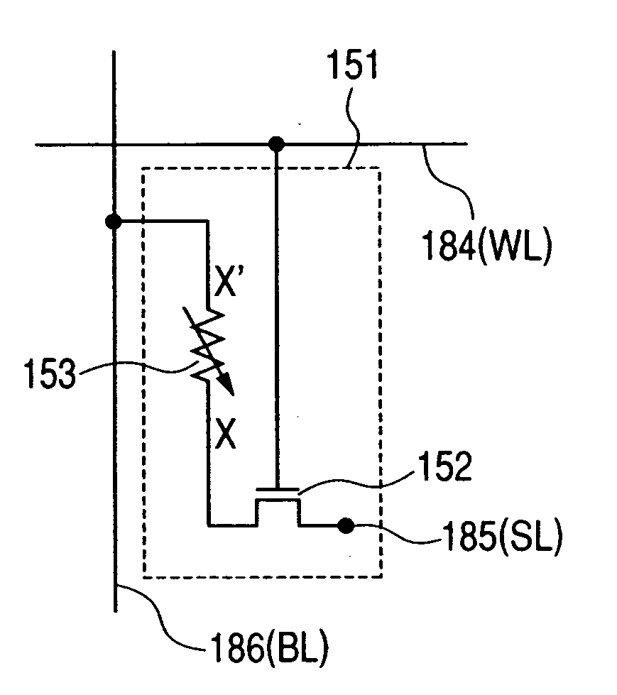
[0052]FIG. 1 and FIGS. 6 to 10 show the semiconductor memory cells and their operational wave forms of the first embodiment of the present invention.

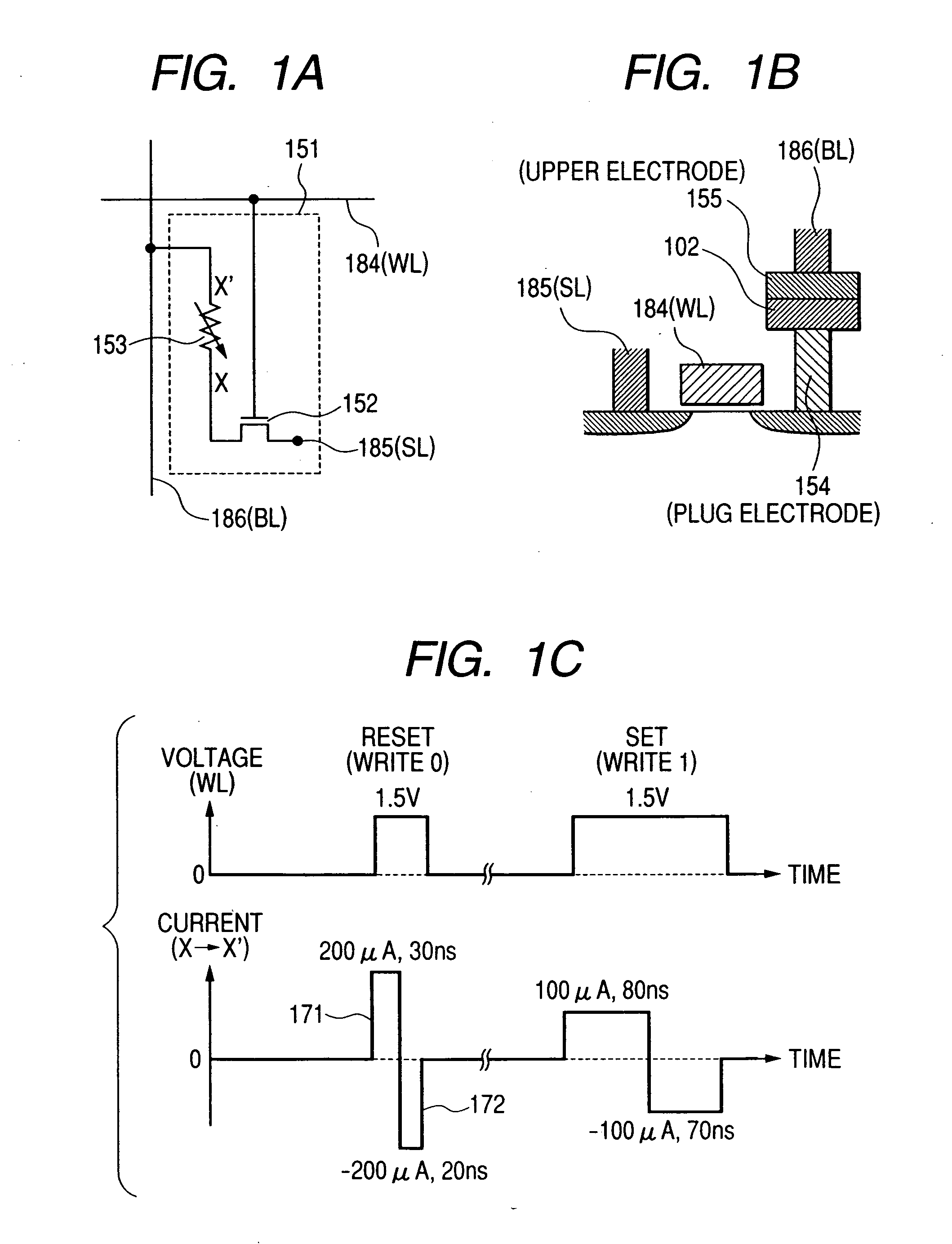
[0053]FIG. 1A shows a memory cell 151 comprising a select element 152 and an information storage section 153. The information storage section 153 has a structure connected to a MOS transistor, i.e., a select element 152, and a source line 185. Of course, another structure is possible, wherein the information storage element is connected to a select element 152 and a bit line 186. In such cases, a current flows from either the bit line 186 or the source linel85 by applying a voltage pulse to the word line 184, to make the select element conductive. FIG. 1B shows a schematic diagram of the memory cell cross-section. The structure of the information storage section 153 is such that a chalcogenide 102 is sandwiched between an upper electrode 155 having a comparatively large contact area with the chalcogenide and a plug electrode 154 having...

second embodiment

[0074] The segregation in the composition of the chalcogenide can be prevented by the present invention disclosed. The chalcogenide, which has been unable to be used since the segregation was easily produced in the prior art, is now available. A criterion for segregation production is a difference in electronegativity between atomic elements composing the storage materials. The composition of the chalcogenide studied mainly as a material for a phase change storage memory is Ge—Sb—Te. As shown in a table in FIG. 12, the electron negativity for Ge is 1.8, for Sb 1.9, and for Te 2.2. Therefore, since a Te element is a relatively negative, it drifts toward the positive electrode. For the electronegativity of the three kinds of element, Ge—Sb—Te, Ge has the minimum value, Te has the maximum, and the difference between the two is 0.3.

[0075] For the chalcogenide with the difference in electronegativity of larger than 0.3 between its composing elements, there was a problem the segregation ...

third embodiment

[0078]FIG. 13 shows a schematic cross sectional view of a storage section of the memory cell according to fourth embodiment of the present invention. An bonding layer 192, a heater layer 193, and the chalcogenide are sandwiched between the electrode 195 and the electrode 196. Here, the bonding layer 192 is arranged not to produce any space between the chalcogenide and the electrode 195 at a memory fabrication process or at the memory operations. The heater layer is arranged to produce joule heat efficiently when the write current flows. With such a structure, since composing atoms from the heater layer or the bonding layer diffuse into the chalcogenide, that the materials with a large diffusion velocity could not be utilized as the heater layer or the bonding layer. However, by the present system of switching the direction of the current, such elements with a large diffusion velocity as Si and C, which could not be used in the prior art, become available to be used for a heater laye...


PUM


Abstract

A semiconductor non volatile memory device capable of multiple write operations with high reliability is implemented. The memory device includes memory cells, each comprising a first electrode, a second electrode, and an information storage section put between the two electrodes, wherein an operation to feed a first pulse current from the first electrode to the second, and another operation to feed a second pulse current from the second electrode to the first. A segregation of composing elements of the information storage section is caused by applying the first pulse, however, the segregation of elements is resolved by applying the second pulse, and the composition of the element recovers to the original state.

Description

CLAIM OF PRIORITY [0001] The present application claims from Japanese application JP 2005-034155 filed on Feb. 10, 2005, and Japanese application JP 2005-116612 filed on Apr. 14, 2005, the contents of which are hereby incorporated by reference into this application. FIELD OF THE INVENTION [0002] The present invention relates to semiconductor integrated circuit devices, and more particularly to an effective technique applicable to the semiconductor integrated circuit devices having discriminator memory cells for stored information utilizing resistance differences, for example, high density integrated memory circuits including the memory cells of phase change materials, logic mix mounted memories wherein a memory circuit and a logic circuit are arranged on the same semiconductor substrate, or analog circuits. Furthermore, the present invention relates in particular to random access memories able to operate under a low voltage, with a high speed, and non-volatile property. BACKGROUND O...

Claims


Application Information

Patent Timeline
Patent Type & Authority Applications(United States)
IPC IPC(8): G11C11/00
CPCG11C13/0004G11C13/0069G11C2013/0073G11C2013/0078G11C2013/0092G11C2213/79G11C13/004G11C13/0061G11C2013/0047
Inventor KUROTSUCHI, KENZOITOH, KIYOOTAKAURA, NORIKATSUOSADA, KENICHI
Owner RENESAS ELECTRONICS CORP
Why Eureka
Try Eureka