Compensation of nonlinearity introduced by dead time in switching output stage

a technology of output stage and compensation, which is applied in the direction of amplifiers, dc amplifiers with modulator-demodulator, amplifiers, etc., can solve the problems of total harmonic distortion, different duty cycle of amplifier output and amplifier input, and adversely affecting specified amplifier performance characteristics

Active Publication Date: 2006-09-21
TEXAS INSTR INC
View PDF7 Cites 23 Cited by
  • Summary
  • Abstract
  • Description
  • Claims
  • Application Information

AI Technical Summary

Benefits of technology

[0013] By varying the duty cycles of the pulses driving the output transistors based on the direction of the residual load current in successive dead time intervals, as described above, the duty cycle of the output pulse can be forced to rema...

Problems solved by technology

The above-described conventional class D amplifier output stage has drawbacks because, in practice, the body diodes of the MOSFET output transistors typically allow a residual load current to flow through the transistors when they are switched off.
Further, because it is not directly related to the input of the ampli...

Method used


Image

  • Compensation of nonlinearity introduced by dead time in switching output stage
  • Compensation of nonlinearity introduced by dead time in switching output stage
  • Compensation of nonlinearity introduced by dead time in switching output stage

Examples


Embodiment Construction

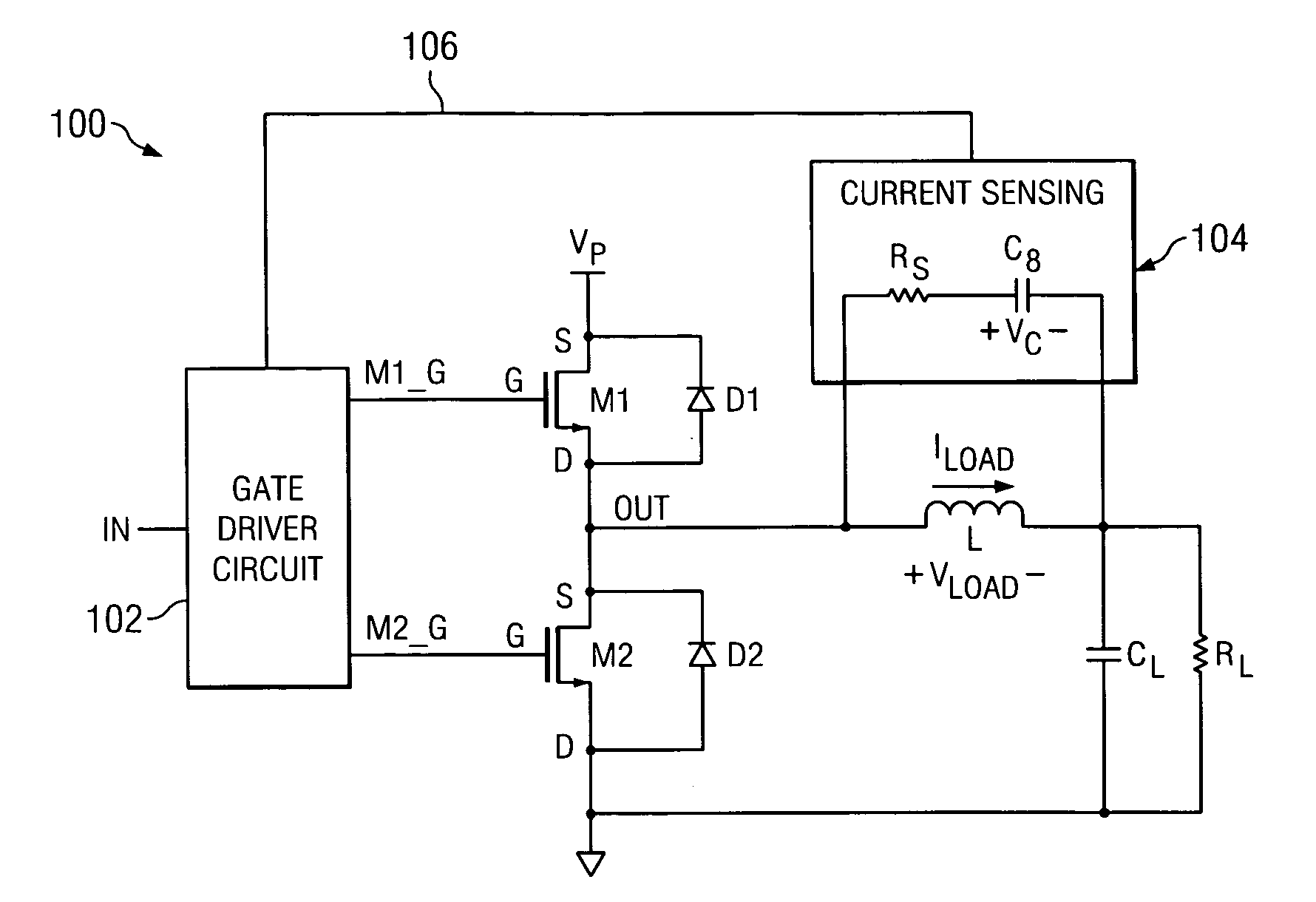
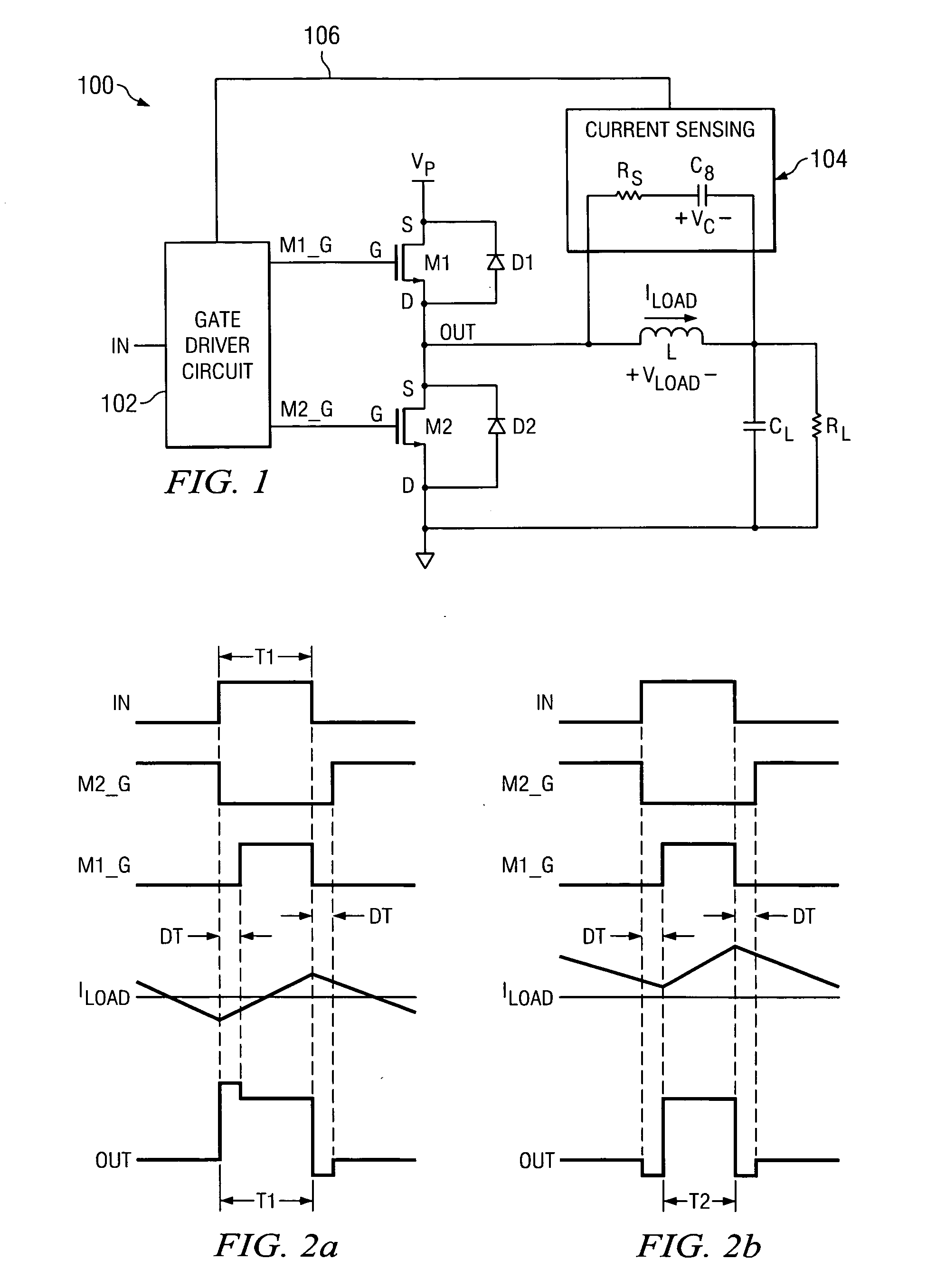
[0021] A method of operating a class D amplifier output stage is disclosed that compensates for nonlinearity introduced by the dead time in the switching of the output stage. FIG. 1 depicts an illustrative embodiment of a class D amplifier output stage 100, in accordance with the present invention. In the illustrated embodiment, the amplifier output stage 100 comprises an input IN, an output OUT, first and second output transistors M1-M2, a gate driver circuit 102, and a current sensing circuit 104, which includes a resistor Rs and a capacitor Cs connected in series across an inductive load L. For example, the output transistors M1-M2 can be respective MOSFET power transistors, or any other suitable type of transistor. In the preferred embodiment, each one of the transistors M1-M2 is an N-type double diffused MOS (DMOS) power transistor.

[0022] As shown in FIG. 1, the output transistors M1-M2 are serially connected between first and second terminals of a power supply. In the illustr...


PUM


Abstract

A method of operating a class D amplifier output stage that compensates for nonlinearity introduced by a residual load current during the dead time in the switching of the output stage. The amplifier output stage includes an input, a gate driver circuit, two output transistors, an output, and a current sensing circuit. The transistors are serially connected between the terminals of a power supply. A residual load current flows through the transistors when they are switched off. The gate driver circuit increases or decreases the duty cycles of signals driving the transistors based on the direction of the residual load current flowing through the transistors, thereby causing the duty cycle of the amplifier output to remain substantially constant and equal to the duty cycle of the amplifier input.

Description

CROSS REFERENCE TO RELATED APPLICATIONS [0001] N / A STATEMENT REGARDING FEDERALLY SPONSORED RESEARCH OR DEVELOPMENT [0002] N / A BACKGROUND OF THE INVENTION [0003] The present application relates generally to output stages of amplifier circuits, and more specifically to a method of compensating for nonlinearity introduced by the dead time in the switching output stage of a class D amplifier. [0004] The output stage of a conventional class D amplifier typically includes two MOSFET transistors serially connected between upper and lower terminals of a power supply. The two transistors operate as switches to commute the output of the amplifier between the voltage levels at the upper and lower power supply terminals, e.g., Vp and GND. Specifically, when an output transistor is switched “on”, the voltage across the transistor is small, e.g., close to 0 volts. Further, when an output transistor is switched “off”, the current through the transistor is essentially zero. As a result, the voltage...

Claims


Application Information

Patent Timeline
IPC IPC(8): H03F3/217
CPCH03F3/217H03F2200/462
Inventor LABBE, ERIC
Owner TEXAS INSTR INC
Why Eureka
Try Eureka