Wafer level package including a device wafer integrated with a passive component

Active Publication Date: 2006-10-05
SKYWORKS SOLUTIONS INC
View PDF48 Cites 59 Cited by
  • Summary
  • Abstract
  • Description
  • Claims
  • Application Information

AI Technical Summary

Benefits of technology

[0008] The present invention is directed to a wafer level package including a device wafer integrated with a passive component. The present invention addresses and resolves the need in the art for a low cost, her

Problems solved by technology
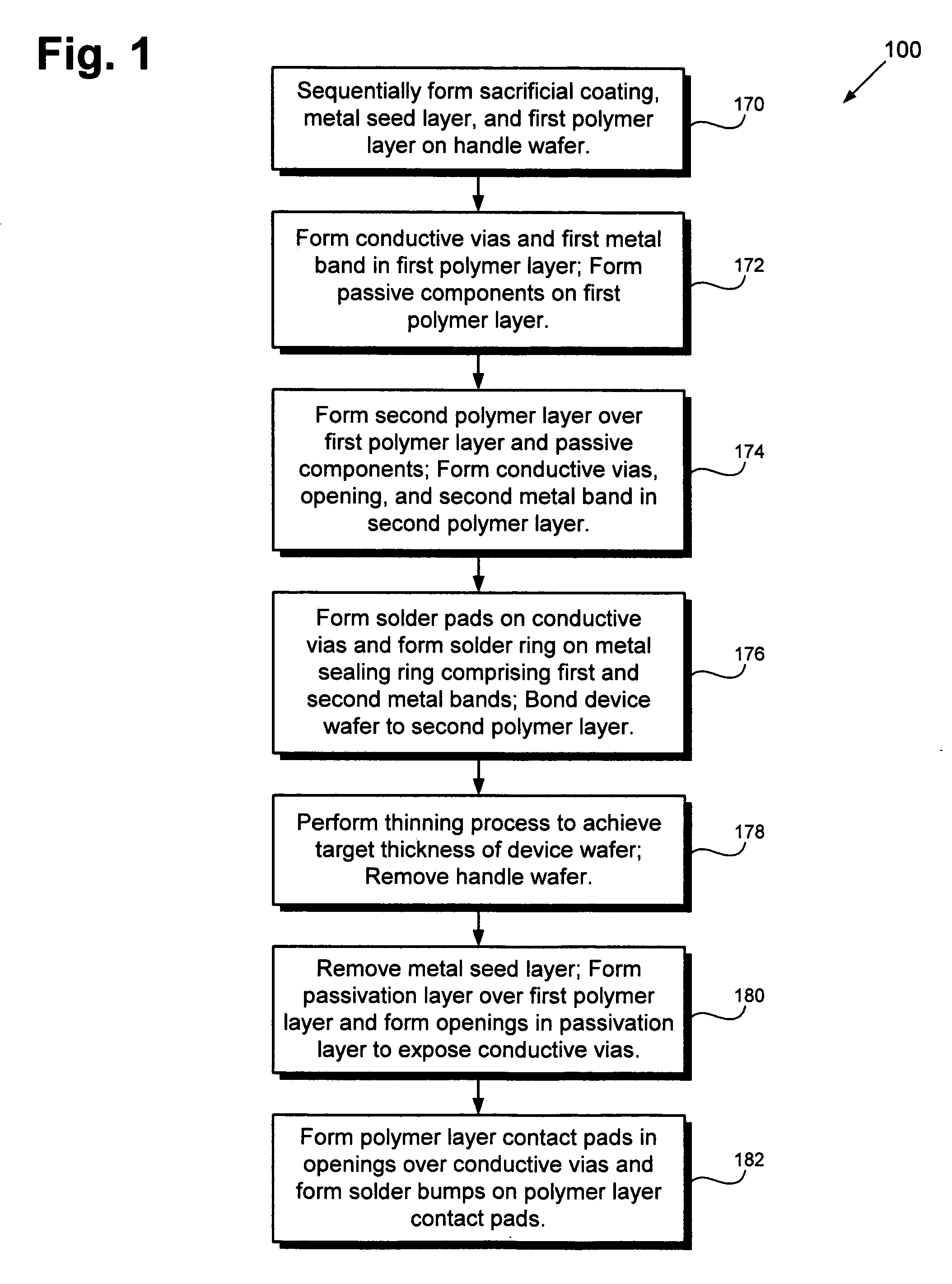
As a result, these electronic devices require smaller, lower cost components, such as integrated circuits (ICs) and Micro-Electro-Mechanical Systems (MEMS) devices.
However, packaging generally consumes between approximately 40.0 percent and approximately 90.0 percent of the total manufacturing cost of the ICs and MEMS devices.
However, most polymer based wafer level packages do not provide a hermetic seal, which is required in certain applications.
However, the use of th

Method used


Image

  • Wafer level package including a device wafer integrated with a passive component
  • Wafer level package including a device wafer integrated with a passive component
  • Wafer level package including a device wafer integrated with a passive component

Examples


Embodiment Construction

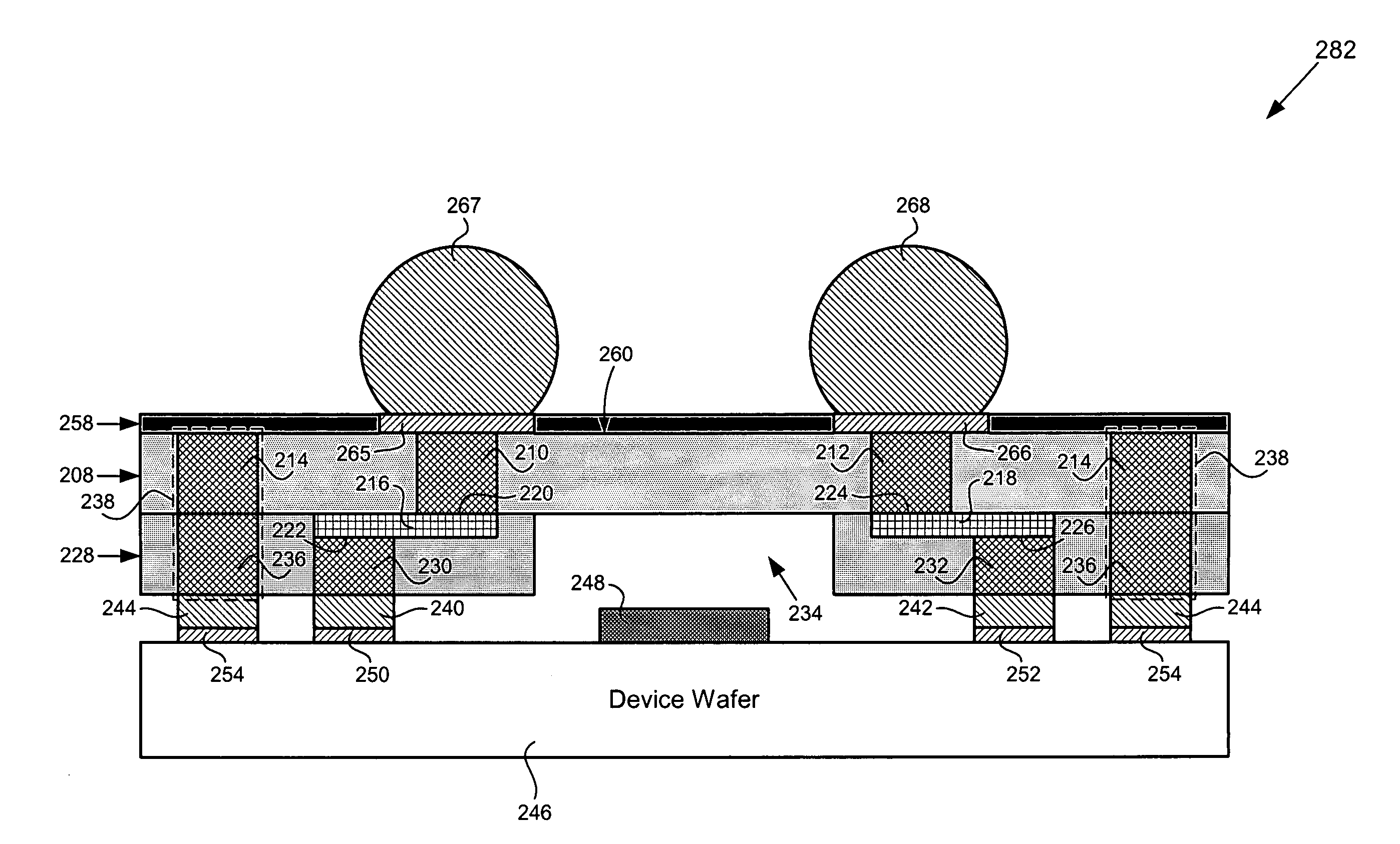
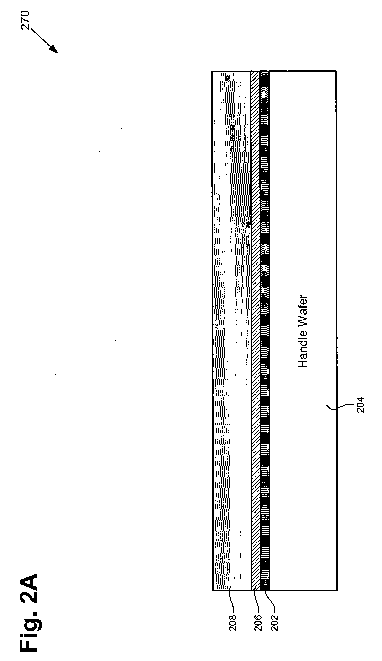
[0020] The present invention is directed to a wafer level package including a device wafer integrated with a passive component. The following description contains specific information pertaining to the implementation of the present invention. One skilled in the art will recognize that the present invention may be implemented in a manner different from that specifically discussed in the present application. Moreover, some of the specific details of the invention are not discussed in order to not obscure the invention. The specific details not described in the present application are within the knowledge of a person of ordinary skill in the art.

[0021] The drawings in the present application and their accompanying detailed description are directed to merely exemplary embodiments of the invention. To maintain brevity, other embodiments of the invention which use the principles of the present invention are not specifically described in the present application and are not specifically il...


PUM


Abstract

According to an exemplary embodiment, a wafer level package includes a device wafer including at least one device wafer contact pad and a device, and where the at least one device wafer contact pad is electrically connected to the device. The wafer level package includes a first polymer layer situated over the device wafer. The wafer level package includes at least one passive component situated over the first polymer layer and having a first terminal and a second terminal. The first terminal of the at least one passive component is electrically connected to the at least one device wafer contact pad. The wafer level package includes a second polymer layer situated over the at least one passive component. The wafer level package includes at least one polymer layer contact pad situated over the second polymer layer and electrically connected to the second terminal of the at least one passive component.

Description

BACKGROUND OF THE INVENTION [0001] 1. Field of the Invention [0002] The present invention is generally in the field of semiconductors. More particularly, the invention is in the field of wafer level packaging. [0003] 2. Background Art [0004] Electronic devices, such as cellular phones and personal digital assistants (PDAs), continue to decrease in size and price and increase in functionality. As a result, these electronic devices require smaller, lower cost components, such as integrated circuits (ICs) and Micro-Electro-Mechanical Systems (MEMS) devices. However, packaging generally consumes between approximately 40.0 percent and approximately 90.0 percent of the total manufacturing cost of the ICs and MEMS devices. As a result, wafer level packaging has emerged as a leading solution to the challenge of providing low cost IC and MEMS device packages that also have a reduced footprint. [0005] In wafer level packaging processes, a layer of polymer material may be used to bond a cap wa...

Claims


Application Information

Patent Timeline
IPC IPC(8): H01L23/48H01L21/44
CPCB81C1/00269H01L21/4857H01L2924/1461H01L21/6835H01L23/49816H01L23/49822H01L24/81H01L2221/68345H01L2224/16H01L2224/81801H01L2924/01078H01L2924/01079H01L2924/04941H01L2924/15184H01L2924/15311H01L2924/19041H01L2924/15151H01L2924/00H01L2924/14H01L2224/05573H01L2224/05568H01L2224/05624H01L2224/05647H01L2924/15159H01L2224/83005H01L2224/32235H01L24/05H01L24/13H01L24/16H01L24/29H01L24/32H01L24/73H01L24/83H01L2221/68327H01L2224/0401H01L2224/04026H01L2224/131H01L2224/16235H01L2224/29011H01L2224/291H01L2224/73103H01L2224/81005H01L2224/81192H01L2224/83192H01L2224/2746H01L2224/1146H01L2224/13109H01L2224/13111H01L2224/13144H01L2224/29109H01L2224/29111H01L2224/29144H01L2224/9211H01L2924/00014H01L2224/0554H01L2924/00012H01L2924/014H01L2924/01047H01L2924/01029H01L2924/0105H01L2224/81H01L2224/83H01L2224/05599H01L2224/0555H01L2224/0556H01L23/48H01L21/44H01L23/12
Inventor GAN, QINGWARREN, ROBERT W.LOBIANCO, ANTHONY J.LIANG, STEVE
Owner SKYWORKS SOLUTIONS INC
Why Eureka
Try Eureka