Dynamically reconfigurable signal processing circuit, pattern recognition apparatus, and image processing apparatus

a signal processing circuit and dynamic reconfiguration technology, applied in the field of dynamic reconfiguration of signal processing circuits, pattern recognition apparatuses, image processing apparatuses, can solve the problems of not ensuring optimal estimation, difficult application of methods, and inability to efficiently sequentially extract plurality of predetermined different geometrical features.

Inactive Publication Date: 2006-10-12
CANON KK
View PDF32 Cites 63 Cited by
  • Summary
  • Abstract
  • Description
  • Claims
  • Application Information

AI Technical Summary

Benefits of technology

[0040] The present invention has been made in consideration of the above-described problems, and has as its object to make it possible to efficiently sequentially extract a plurality of predetermined different geometrical features from time-serially input image data.
[0041] It is another object of the present invention to efficiently and stably execute different spatial filter processing operations for a sensed image by making a temporally modulated spatial filter output synchronous with the sensor output timing.
[0042] It is still another object of the present invention to make it possible to control the interconnection structure between arithmetic processing blocks and a signal processing function including modulation by the arithmetic processing blocks and to construct various circuits by a small number of basic circuit arrangements.
[0043] It is still another object of the present invention to make it possible to switch the circuit arrangement and circuit characteristic of an arithmetic processing block and commonly use it for a plurality of signal processing operations, thereby reducing the circuit scale.
[0044] It is still another object of the present invention to make it possible to omit unnecessary switching of the circuit arrangement and circuit characteristic in switching the function of an arithmetic processing block, thereby reducing power consumption.

Problems solved by technology

However, in the above prior art, a plurality of predetermined different geometrical features cannot be efficiently sequentially extracted from time-serially input image data by the single circuit.
However, of the above prior arts, the arrangement disclosed in Japanese Patent Laid-Open No. 11-15945 does not explain how to integrate matching results when object models have a plurality of categories, and which local model yields matching results to be integrated.
In this prior art, confidence degrees for the presence of features by a non-additive measure are integrated on the basis of, e.g., the Dempster-Shafer theory, though it does not guarantee optimum estimation.
In addition, if the size of an object in an image is different from that of an object model, or if a plurality of objects with different sizes simultaneously exist, the method is hard to apply.
The arrangement of the pattern recognition apparatus disclosed in Japanese Patent Laid-Open No. 6-176158 cannot improve the memory efficiency or reduce the circuit scale.
In any of the above prior arts, hence, the number of elements in the lower layer increases depending on the size of an input image, resulting in an increase in circuit scale.
Hence, only with the FPGA, analog parallel arithmetic processing of a neural circuit network or like cannot be implemented.
No. 11-168185 to a neural circuit network, when the number of neural elements increases, the number of input / output terminals exponentially increases, resulting in difficulty in handling.
For this reason, in principle, it is difficult to set an arbitrary interconnection structure, and a special process for mounting the elements on a stacked substrate is required.
However, it is difficult to implement a large-scale parallel hierarchical processing circuit.
In the hierarchical neural network disclosed in Japanese Patent No. 2679730, since no means for variably arbitrarily controlling the inter-layer connection is prepared, the number of types of processing that can be substantially realized is considerably limited.
For this reason, the scale of the circuit component (analog processing cell) becomes very large, and therefore, the total circuit area inevitably increases.
Additionally, in a structure in which analog processing units each incorporating a multiplexer and demultiplexer are arrayed on a two-dimensional plane, it is difficult to realize an arbitrary connection structure and, more particularly, hierarchical connection.

Method used


Image

  • Dynamically reconfigurable signal processing circuit, pattern recognition apparatus, and image processing apparatus
  • Dynamically reconfigurable signal processing circuit, pattern recognition apparatus, and image processing apparatus
  • Dynamically reconfigurable signal processing circuit, pattern recognition apparatus, and image processing apparatus

Examples


first embodiment

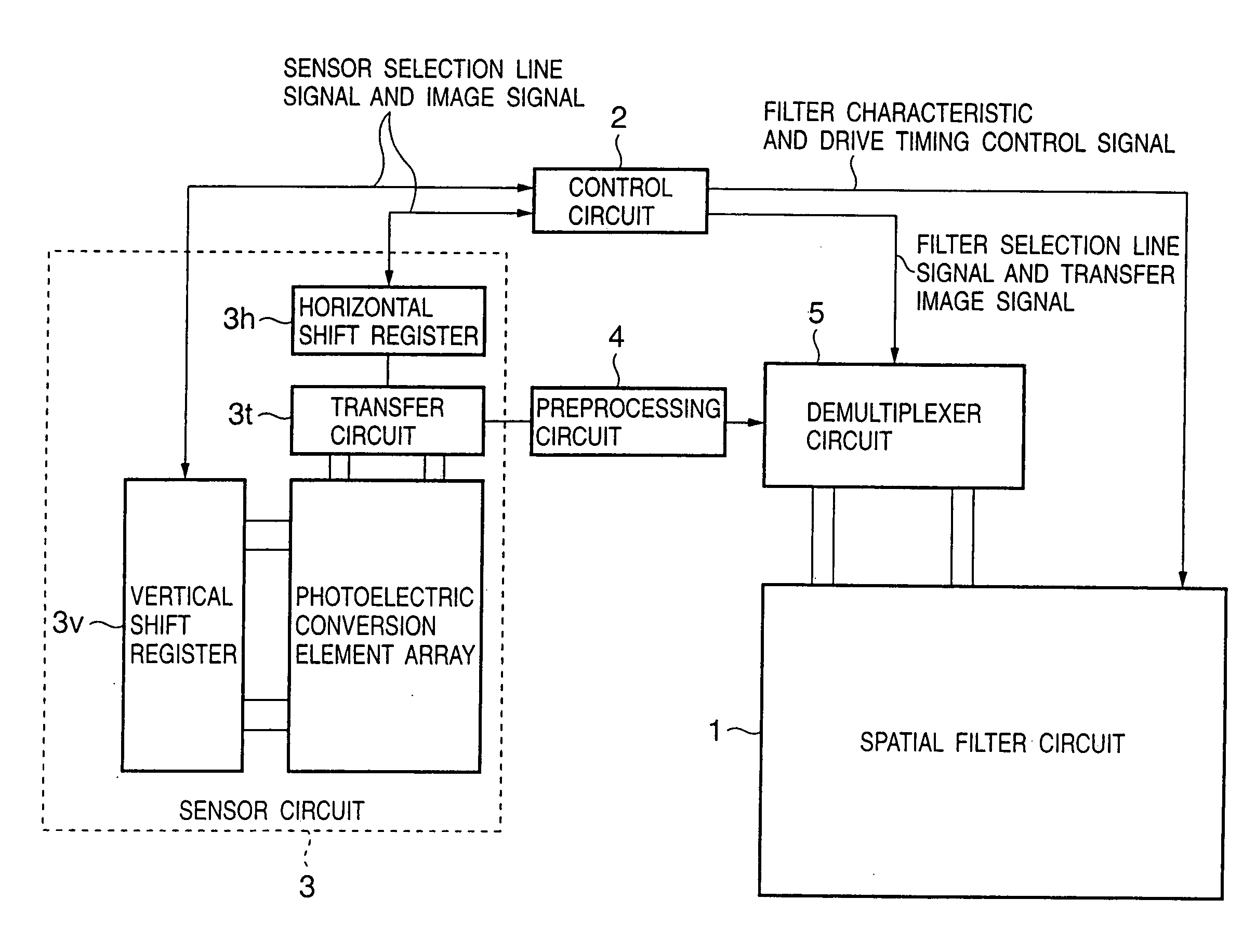
[0110]FIG. 1 is a block diagram showing the overall arrangement of an image sensing signal processing circuit according to the first embodiment.

[0111] Referring to FIG. 1, a spatial filter circuit 1 time-serially executes predetermined spatial filter operations having different characteristics at points corresponding to the respective pixel positions, on the sensor, of a video signal input from a sensor circuit 3. The spatial filter circuit 1 has a function of time-serially extracting different geometrical image features for regions with a predetermined size around the respective points of a video signal.

[0112] A control circuit 2 outputs a predetermined read control pulse signal to the sensor circuit 3 in accordance with a predetermined timing and also outputs a timing pulse signal synchronous with the read control pulse signal to the spatial filter circuit 1, thereby synchronously processing the output from the sensor circuit 3 and the spatial filter circuit 1, as will be descri...

second embodiment

[0166]FIG. 6 is a block diagram showing the arrangement of main part of the second embodiment. According to this arrangement, the memory element Cm at the input unit of the spatial filter circuit element shown in FIG. 3 is unnecessary. Of a sensor circuit output, a necessary portion corresponding to a predetermined spatial filter circuit element to be time-serially accessed is temporarily recorded in a block memory 6. Then, pixel data in the block memory 6 are read out at once (time-serially in the case of the first embodiment where the memory element Cm is used in the circuit shown in FIG. 3) as voltage signals, and the above-descried spatial filter processing is performed.

[0167] In this embodiment, a control circuit 2 sends, of spatial filter characteristic parameters (m,n), a scale control signal corresponding to the scale parameter m to a sensor circuit 3 side together with an address selection signal. The horizontal and vertical selection circuits (3h and 3v) in the sensor cir...

third embodiment

[0172]FIG. 7 shows the arrangement of main part of the third embodiment. Timing control characteristic of a sensor circuit 3, i.e., the modulation timing control on a spatial filter circuit 1 side is done using a read control signal used in a normal CMOS sensor. In this case, interlaced read control as in the first embodiment is done.

[0173] With this arrangement, the read timing control about the CMOS sensor circuit 3 or the internal interconnection of a transfer circuit 3t or the like need not be changed. Hence, stable spatial filtering operation can be executed using an existing CMOS sensor chip or the like.

[0174] A control circuit 2 receives selection line signals in the sensor read mode to obtain the address information of an image signal and executes transfer control of the image signal to a spatial filter circuit element at a corresponding position.

[0175] At this time, characteristic control signals for circuit elements (resistors and transconductance amplifiers) shown in F...


PUM


Abstract

A plurality of signal processing functions are achieved with the same arithmetic processing circuit by controlling wiring arrangements or signal modulation in accordance with a predetermined arrangement control signal that is output based on circuit arrangement information read from a circuit arrangement information storage unit. Hierarchical parallel processing is realized with small-scale circuit configuration. Further, detection of a predetermined feature and integration of the detection results can be efficiently performed.

Description

FIELD OF THE INVENTION [0001] The present invention relates to an image processing apparatus and, more particularly, to a circuit preferable for sensor signal processing of processing an image sensing signal from an image sensor such as a CMOS sensor and executing image processing such as recognition, detection, extraction, and the like of an object. [0002] The present invention also relates to a pattern recognition processing apparatus using parallel calculations. [0003] The present invention also relates to an analog-digital mixed type signal processing circuit capable of changing a circuit arrangement in accordance with processing contents. [0004] The present invention also relates to an analog-digital mixed or merged type signal processing circuit capable of changing the circuit arrangement in accordance with processing contents and a pattern recognition apparatus using the signal processing circuit. BACKGROUND OF THE INVENTION [0005] Conventionally, as image sensors having an i...

Claims


Application Information

Patent Timeline
Patent Type & Authority Applications(United States)
IPC IPC(8): G06K9/00G06K9/46G06K9/66
CPCG06K9/00281G06K9/4628G06K9/00973G06N3/049G06N3/063G06V40/171G06V10/94G06V10/454
Inventor MATSUGU, MASAKAZUMORI, KATSUHIKONOMURA, OSAMU
Owner CANON KK
Why Eureka
Try Eureka