
Eureka
For R&D, Eureka makes reading and utilizing patents & technical documents easy.
Eureka AIR
Designed for self-driven R&D workflows. Generate viable solutions, solve complex R&D challenges, empower your innovation with AI.

Eureka Materials
Designed for material experts only. Revolutionize your material R&D, from search, analyze, to developing new materials.

TechResearch
Generate reliable direction feasibility study reports for your R&D in just a few steps.

TechSeek
Discover and master advanced knowledge NOW. Basics, ideas, possibilities, all at once.

TechMind
As an expert in R&D Theories, TechMind can generates customized viable solutions instantly.

TechRisk
Analyze your overall solution with one click, know your potential R&D risks in advance.

TechMonitor
Get weekly tech updates, stay abreast of the latest tech innovations and key insights.
Technique for manufacturing micro-electro mechanical structures
- Summary
- Abstract
- Description
- Claims
- Application Information
AI Technical Summary
Problems solved by technology
Method used
Image

Examples
Embodiment Construction
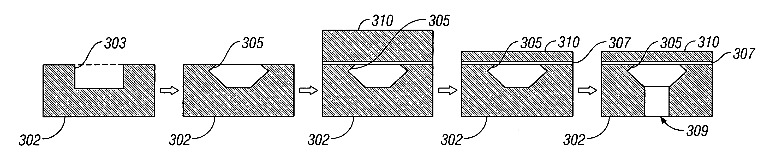
[0019] According to the present invention, a lower cost micro-electro mechanical (MEM) pressure sensor, e.g., a single-crystal silicon pressure sensor, is produced that has a reduced size, while providing a rugged membrane. As is discussed above, the area required for a sensor die has typically been determined by the processes that are used to micromachine a membrane (diaphragm) of the sensor. According to the present invention, a membrane is formed by a thin silicon layer that is left after thinning of an active wafer. Furthermore, if desired, access to the back of the membrane can readily be provided by a partial etch of the handling wafer, before bonding, followed by a deep reactive ion etch (DRIE) from the back of the handling wafer. In this manner, the area occupied by the etched hole is reduced, while the membrane size is readily controlled.
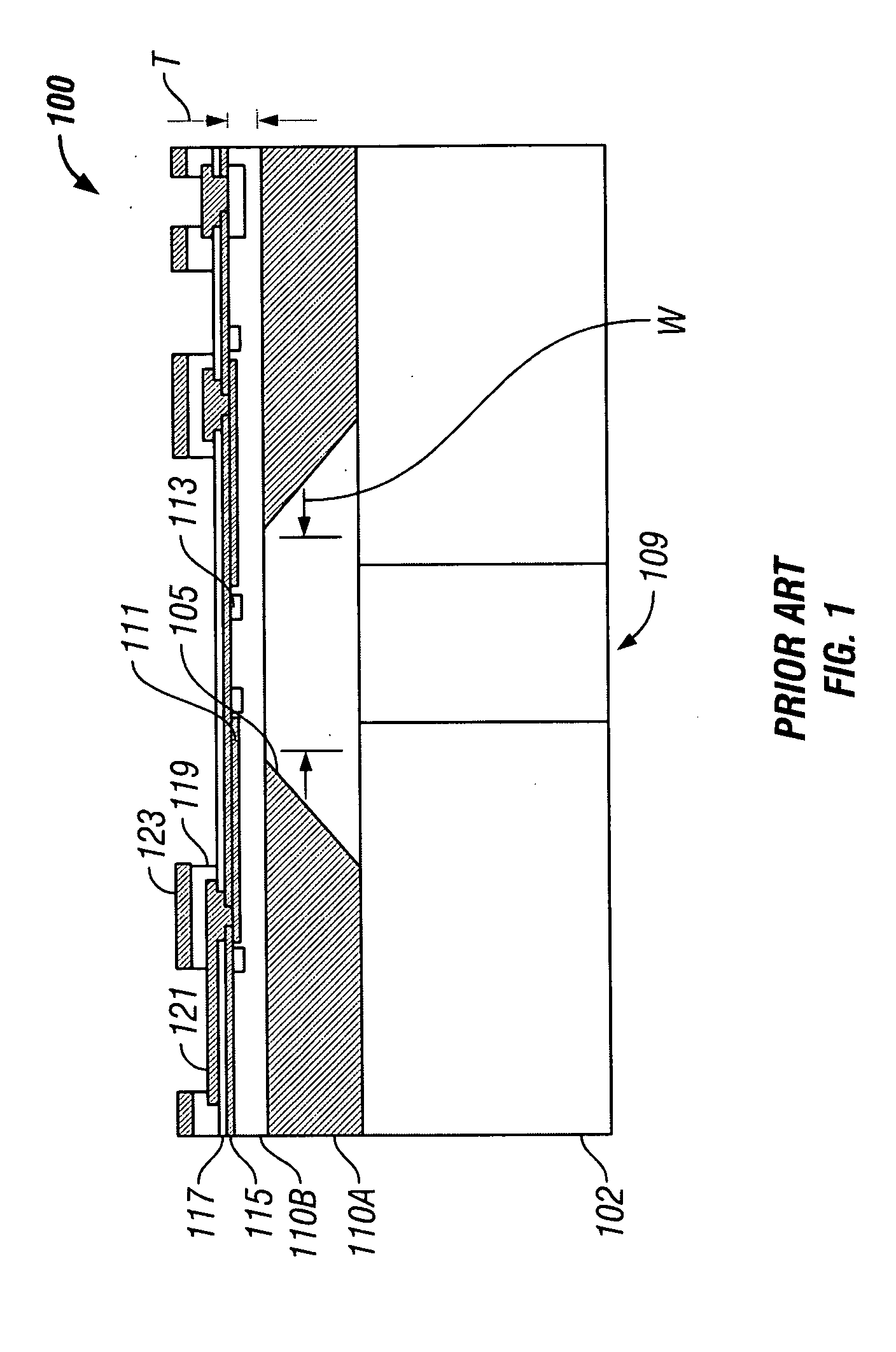
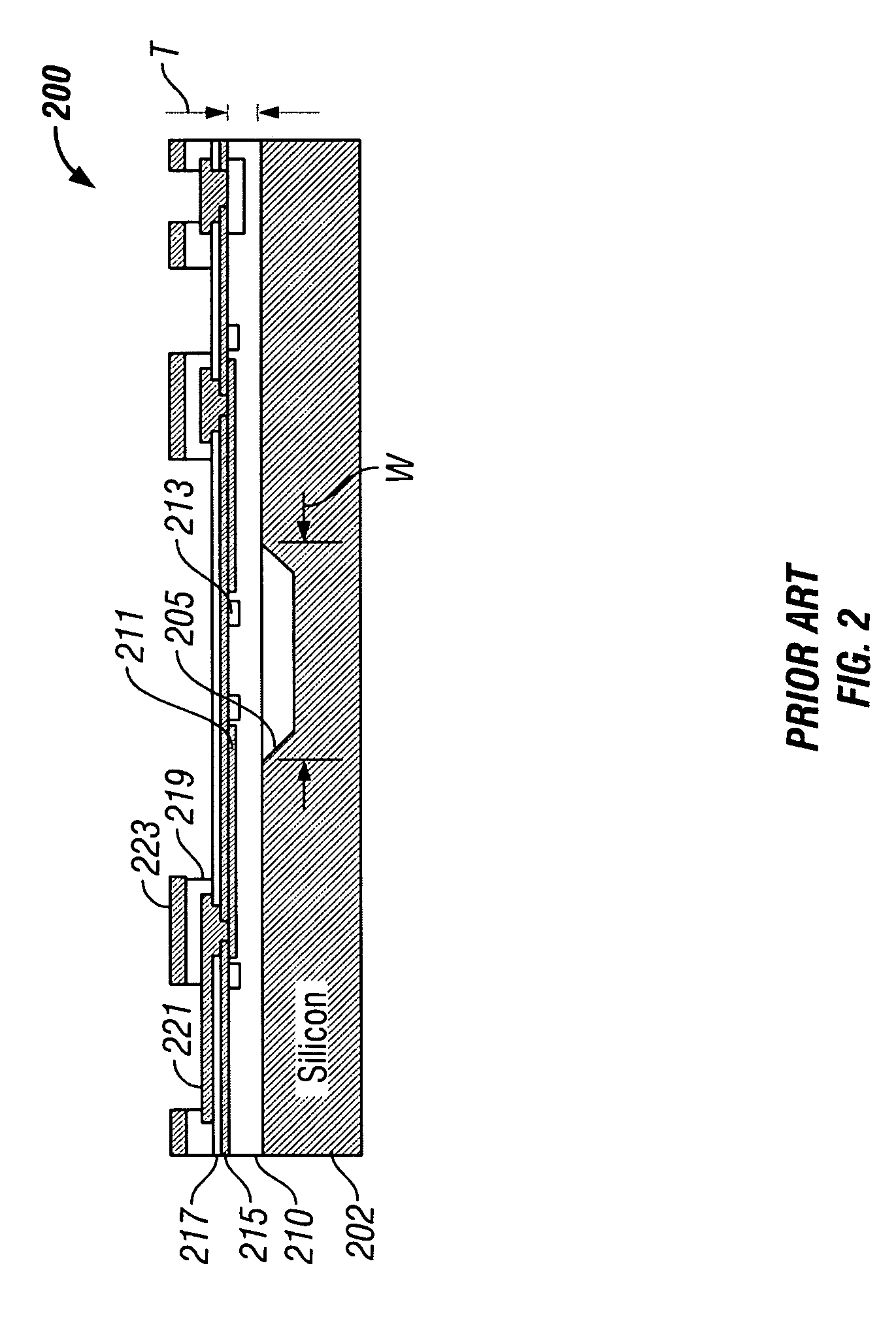
[0020] As is mentioned above, a pressure sensor manufactured using a backside etch process has provided a relatively large size sensor wi...
PUM
| Property | Measurement | Unit |
|---|---|---|
| Length | aaaaa | aaaaa |
| Length | aaaaa | aaaaa |
| Thickness | aaaaa | aaaaa |
Abstract
Description
Claims
Application Information
 - R&D Engineer
- R&D Manager
- IP Professional
- Industry Leading Data Capabilities
- Powerful AI technology
- Patent DNA Extraction
Browse by: Latest US Patents, China's latest patents, Technical Efficacy Thesaurus, Application Domain, Technology Topic, Popular Technical Reports.
© 2024 PatSnap. All rights reserved.Legal|Privacy policy|Modern Slavery Act Transparency Statement|Sitemap|About US| Contact US: help@patsnap.com