

Lens and optical system
a technology of optical systems and lenses, applied in the field of lenses and optical systems, can solve problems such as limited image resolution
- Summary
- Abstract
- Description
- Claims
- Application Information
AI Technical Summary
Problems solved by technology
Method used
Image

Examples
first embodiment
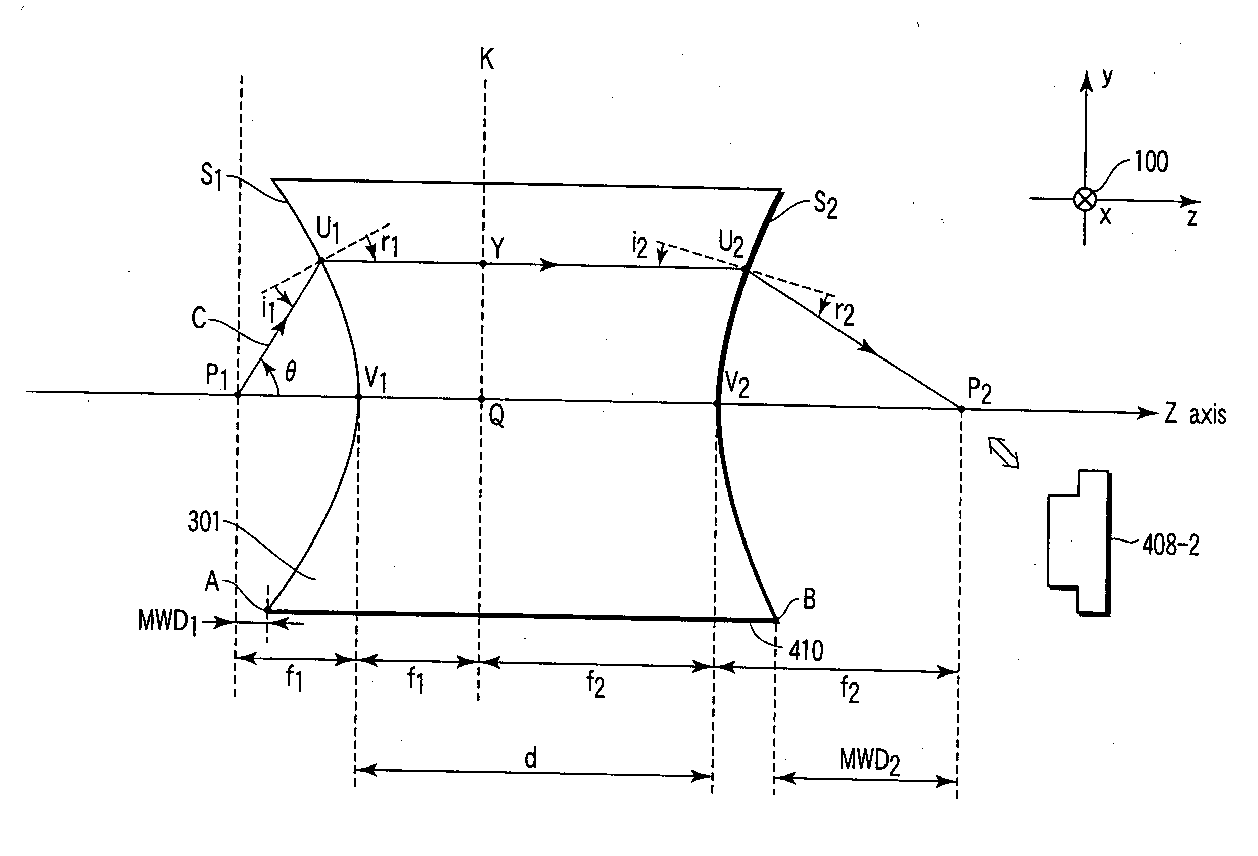
[0052]FIG. 1 is a view for explaining the present invention. A lens 410 is formed of a negative refractive index medium 301 comprising curved surfaces S1 and S2 as two optical surfaces. In the case of three dimensions, S1 and S2 are formed in the shape of a rotational paraboloid with a Z axis being a rotary axis. These curved surfaces are arranged such that convex surfaces sharing two axes are opposed to each other. In the case of two dimensions, S1 and S2 are provided as parabolas with the Z axis being an axis.
[0053] Hereinafter, although a description will be given with respect to the case of three dimensions, this description is also applicable to the case of two dimensions. In FIG. 1, a positive direction of an x axis is provided as a direction oriented from top to bottom of paper. A symbol designated by reference numeral 100 represents this direction. A focal point of a paraboloid of the curved surface S1 is defined as P1. A focal point of a paraboloid of the curved surface S2 ...
second embodiment
[0108]FIG. 3 is a view for explaining the present invention, and shows a microscope 422 using a lens 410. The light beams emitted from a light source 303 are focused by an illumination lens 423, and illuminate a sample 307. The light beams scattered from the sample 307 are formed as an image by the lens 410 having a function as an objective lens, an optical path thereof is bent on a mirror 424, and an actual image is produced on an I.P. The sample 307 corresponds to P1, and the I.P. corresponds to P2. Then, the image is magnified by an ocular lens 308, and a magnified image can be seen by an eye 309.
[0109] Alternatively, a magnified image can be picked up by a television camera 425 provided rearward of the ocular lens 308. Here, reference numeral 426 denotes an image pickup lens, 408 denotes a solid state image pickup element, 427 denotes an electronic circuit, and 428 denotes a display device.
[0110] The ocular lens 308 and the image pickup lens 426 are made of a medium having a po...
third embodiment
[0117]FIG. 4 is a view for explaining the present invention. In the figure, an illumination optical system 413 uses a lens 412 formed of a negative refractive index medium 301. A left side face 413 of the lens 412 is provided as a rotational paraboloid, and a right side face 414 of the lens 412 is provided as a flat surface. An axis of the illumination optical system 413 is provided as a Z axis.
[0118] A light source 415 is arranged at a focal point P1 of the illumination optical system 413, and the light beams emitted from the light source 415 are refracted by the illumination optical system 413, and are emitted as light beams parallel to the Z axis. In this optical system, a magnification β is infinitely large. Then, image formation with no aberration can be carried out in an infinitely telescopic manner.
[0119] As compared with a conventional illumination system using a reflection cover, a light source itself does not block an optical path, and an efficient illumination optical sy...
PUM
 Abstract
Description
Claims
Application Information