
Multi-bit virtual-ground NAND memory device

Inactive Publication Date: 2006-11-02
POLARIS INNOVATIONS
View PDF10 Cites 22 Cited by
  • Summary
  • Abstract
  • Description
  • Claims
  • Application Information

AI Technical Summary

Benefits of technology

[0007] In one aspect, the present invention presents a charge-trapping memory device, including an arra

Problems solved by technology

The shrinkability of 2-bit / cell charge-trapping memory devices is essentially limited by two restrictions.
However, this is not actually possible if the usual read / write operation is implemented in the memory device, since the memory cells of a string can only be addressed via further memory cells that are connected in series.

Method used


Image

  • Multi-bit virtual-ground NAND memory device
  • Multi-bit virtual-ground NAND memory device
  • Multi-bit virtual-ground NAND memory device

Examples


first embodiment

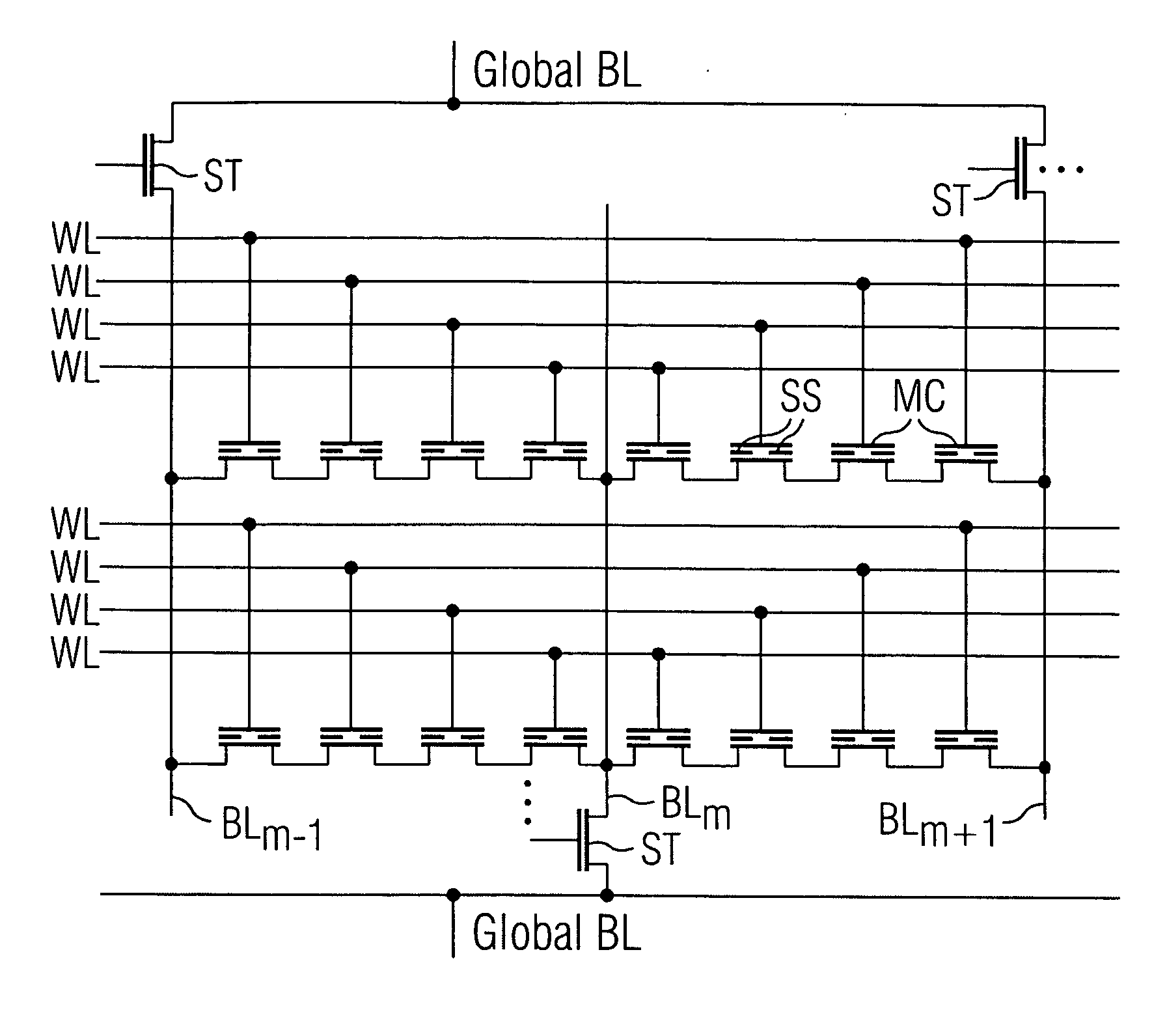
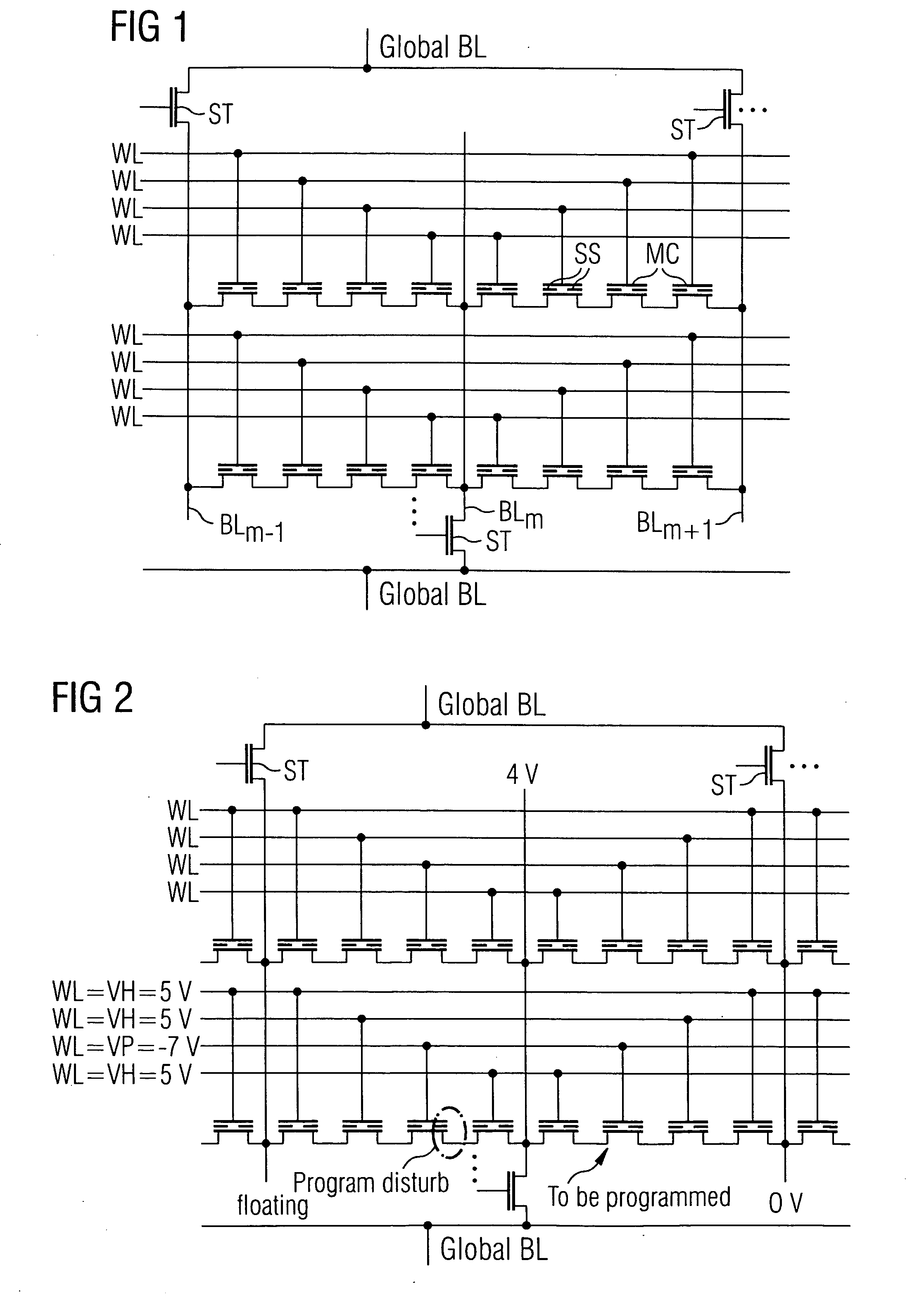
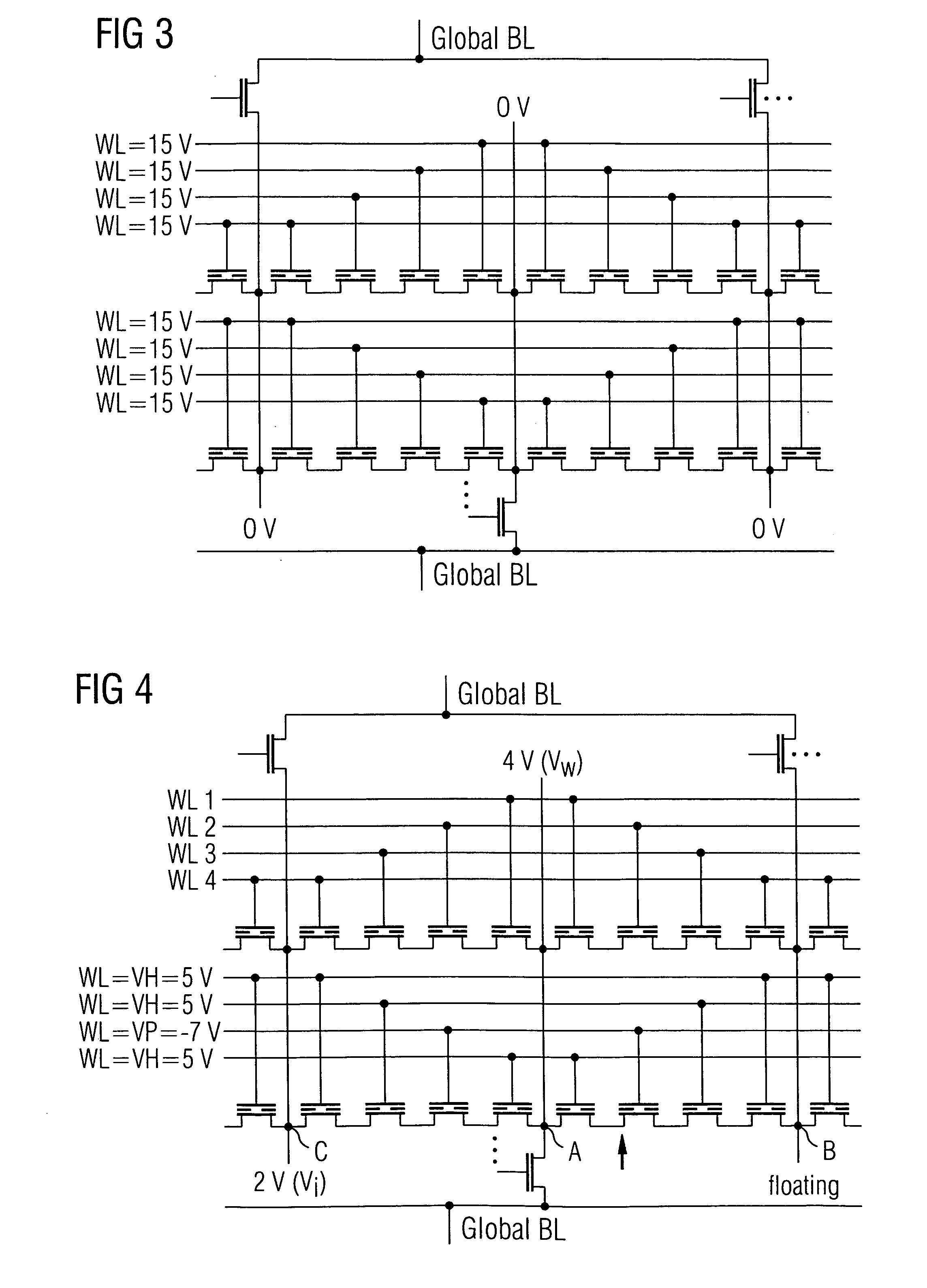
[0053] In this memory device, charge-trapping memory cells are arranged and connected as a virtual-ground NAND array. FIG. 1 shows a circuit scheme of a section of a This scheme shows a number of memory cells MC that are part of the memory cell array. Every memory cell MC is a charge-trapping memory cell, which comprises two storage sites SS adjacent to both source / drain connections. In FIG. 1, the memory cells are drawn on a horizontal line, which does not represent the actual physical arrangement of the memory cells within the array. The wordlines WL run along the rows of memory cells, and the bitlines BL run along the columns, transversely to the wordlines. The memory cells shown in the section of FIG. 1, which are situated between bitlines BLm−1 and BLm, all belong to the same column of memory cells. Their sequence along the column can be inferred from their connections to the drawn wordlines. The bitlines are connected to either of two global bitlines by means of selection tra...

second embodiment

[0066]FIG. 10 is a plan view according to FIG. 8 for an embodiment according to the circuit scheme of FIG. 7. In this embodiment, the bitlines BL run in zigzag fashion essentially along the columns. The bitline connections BC along one single bitline are alternatingly connected to the source / drain connections of two adjacent columns of memory cells. The sequence of NAND chains, which are shown on horizontal straight lines in FIG. 6, is again highlighted by the hatching. The source / drain connections at the ends of the NAND chains of this sequence of the second embodiment do not coincide, but are electrically connected by the bitlines. This can be seen from the double arrows on the right side. The double arrows show the sequence of NAND cells, which are arranged along the double arrows that are directed vertically, and which are connected by sections of the bitlines, which are indicated by the slightly tilted double arrows. The pitch p of the memory cell array and the pitch p′ of the ...


PUM


Abstract

An array of charge-trapping multi-bit memory cells is arranged in a virtual-ground NAND architecture. The memory cells are erased by Fowler-Nordheim tunneling of electrons into the memory layers. The write operation is effected by hot hole injection. A write voltage is applied by a bitline to two NAND chains in series. The subsequent bitline on the side of the memory cell to be programmed is maintained on floating potential, whereas the bitline on the other side is set to an inhibit voltage, which is provided to inhibit a program disturb of an addressed memory cell which is not to be programmed. This virtual-ground NAND architecture of charge-trapping memory cells enables an increased storage density.

Description

TECHNICAL FIELD [0001] This invention concerns virtual-ground NAND memory devices comprising multi-bit charge-trapping memory cells. BACKGROUND [0002] Charge-trapping memory devices, which comprise a memory layer sequence of dielectric materials provided for charge-trapping to program the memory cell, especially SONOS memory cells comprising oxide-nitride-oxide layer sequences as storage medium, are usually programmed by channel hot electron injection. Charge-trapping memory cells can be structured to enable the storage of two bits of information in each memory cell. U.S. Pat. No. 5,768,192 and U.S. Pat. No. 6,011,725, both of which are incorporated herein by reference, disclose charge-trapping memory cells of a special type of so-called NROM cells, which can be used to store bits of information both at the source and at the drain below the respective gate edges. The programmed cell is read in reverse mode to achieve a sufficient two-bit separation. Erasure is performed by hot hole ...

Claims


Application Information

Patent Timeline
IPC IPC(8): G11C17/00
CPCG11C16/0475H01L27/11568H01L27/115G11C16/0483H10B43/30H10B69/00G11C16/0491
Inventor MIKOLAJICK, THOMASWILLER, JOSEFLIAW, CORVIN
Owner POLARIS INNOVATIONS
Learn More