

Semiconductor laser device
a semiconductor laser and surface-emitting technology, which is applied in semiconductor lasers, laser details, electrical equipment, etc., can solve the problems of reducing the gain at the resonant wavelength, deteriorating the characteristics of the vcsel, and insufficient temperature characteristics of the semiconductor laser in an application under environment conditions, and achieves excellent temperature characteristics, low threshold current, and high light-emission recombination efficiency
- Summary
- Abstract
- Description
- Claims
- Application Information
AI Technical Summary
Benefits of technology
Problems solved by technology
Method used
Image

Examples
embodiment 1
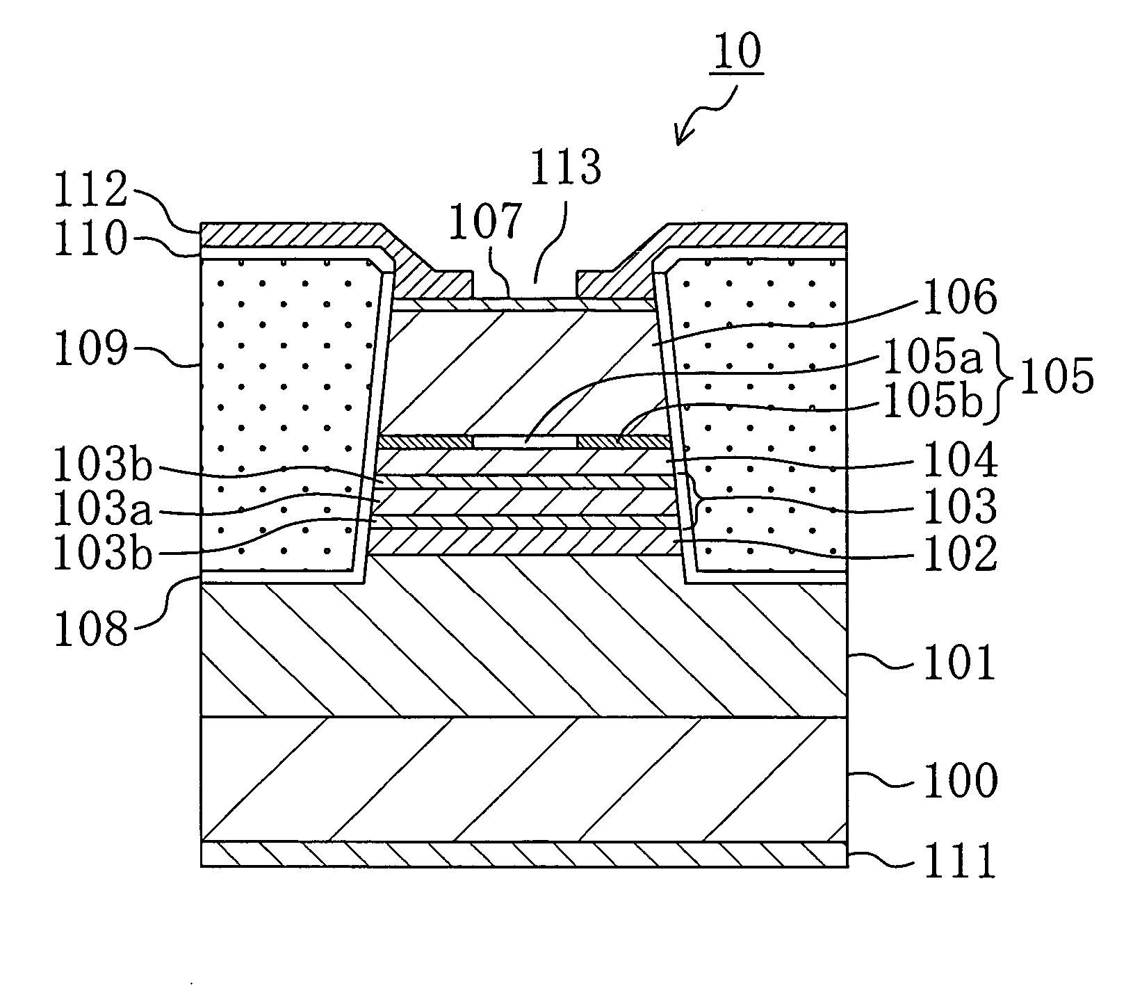
[0041]FIG. 1 is a cross-sectional view illustrating a semiconductor laser device according to a first embodiment of the present invention.
[0042] As illustrated in FIG. 1, in a semiconductor laser device 10 according to the first embodiment, an n-type lower multilayer reflector 101, a lower spacer layer 102, an active layer 103, an upper spacer layer 104, a current confinement layer 105, a p-type upper multilayer reflector 106 and a p-type contact layer 107 are laminated in this order on a substrate 100 of n-type GaAs.
[0043] The n-type lower multilayer reflector 101 is a multilayer film formed by alternately stacking n-type Al0.12Ga0.88As layers and n-type Al0.90Ga0.10As layers. The thickness of each layer is λ / 4 n (λ: a laser oscillation wavelength, n: a refractive index of a medium) and the n-type Al0.12Ga0.88As layers and the n-type Al0.90Ga0.10As layers are laminated by 34.5 cycles (34.5 pairs). Each of the top and bottom layers of the n-type lower multilayer reflector 101 is a...
embodiment 2
[0072] Hereinafter, a semiconductor laser device according to a second embodiment of the present invention will be described with reference to the drawings. Part of the cross-sectional structure of the semiconductor laser device of this embodiment common to that of the first embodiment has been already described in the first embodiment. In this embodiment, only part of the semiconductor laser device of the second embodiment different from that of the first embodiment will be described.
[0073]FIG. 7 is a cross-sectional view illustrating the semiconductor laser device of the second embodiment.
[0074] As illustrated in FIG. 7, the semiconductor laser device of this embodiment is different from that of the first embodiment in that a buffer layer 116 of AlInP is formed between an upper spacer layer 104 of AlGaInP and a current confinement layer 105.
[0075] In crystal growth of an AlGaAs layer on an AlGaInP layer containing a different Group-V element, the Ga content of the AlGaInP layer...
embodiment 3
[0081] Hereinafter, a semiconductor laser device according to a third embodiment of the present invention will be described with reference to the drawings. Part of the cross-sectional structure of the semiconductor laser device of this embodiment common to that of the first embodiment is already described in the first embodiment. In this embodiment, only a part of the semiconductor laser device of the third embodiment different from that of the first embodiment will be described.
[0082]FIG. 9 is a cross-sectional view illustrating the semiconductor laser device of the third embodiment.
[0083] As illustrated in FIG. 9, the semiconductor laser device of the third embodiment is different from that of the first embodiment in that a mesa structure including a current confinement layer 105, a p-type upper multilayer reflector 106 and a p-type contact layer 107 is formed and a portion of an n-type lower multilayer reflector 101, a lower spacer layer 102, an active layer 103 and an upper sp...
PUM
 Abstract
Description
Claims
Application Information