GaN-base double-blue-light wavelength luminescent device and preparation method thereof

A blue light and wavelength technology, applied in semiconductor devices, electrical components, circuits, etc., can solve the problems of shortening the service life of LEDs, difficulty in InGaN films, uneven luminous intensity, etc., to improve the lumen efficiency and the uniformity of electron hole concentration. Effect

Inactive Publication Date: 2012-02-08
SOUTH CHINA NORMAL UNIVERSITY
View PDF5 Cites 8 Cited by
  • Summary
  • Abstract
  • Description
  • Claims
  • Application Information

AI Technical Summary

Problems solved by technology

[0005] 1. Due to the effective mass of GaN-based material holes (1.1 m 0 ) higher than the effective mass of the electron (0.2 m 0 ), therefore, it is easier for electrons to pass through the active layer into the quantum well layer on the top of the active layer, and even overflow the active layer into the p-GaN layer. On the contrary, it is more difficult for the holes to reach the quantum well near the n-GaN side of the active layer
The use of the AlGaN electron blocking layer is intended to block the overflow of electrons and improve the recombination rate of carriers, but it further blocks the injection of holes.
[0006] 2. The p-AlGaN electron blocking layer reduces the hole injection efficiency, resulting in uneven electron-hole concentration distribution in the active region of the single-wavelength LED. Luminous intensity is more uneven
[0009] 5. Due to the low hole concentration of the p-AlGaN layer, the resistance near the interface between the p-type layer and the pn junction is very large, which will generate a lot of heat when the LED is working, resulting in an increase in the junction temperature of the LED and shortening the service life of the LED
However, for GaN-based light-emitting devices, the luminous efficiency is generally higher in the range of 400-500 nm. As the emission wavelength increases toward the green light direction, the luminous efficiency of GaN-based LEDs gradually decreases, mainly because of the realization of high In Composition of InGaN thin films is extremely difficult

Method used


Image

  • GaN-base double-blue-light wavelength luminescent device and preparation method thereof
  • GaN-base double-blue-light wavelength luminescent device and preparation method thereof
  • GaN-base double-blue-light wavelength luminescent device and preparation method thereof

Examples


Embodiment Construction

[0032] The following descriptions are given to enable those skilled in the art to make and use the invention, and are provided in the context of specific applications and needs. Various modifications to the disclosed embodiments will be readily apparent to those skilled in the art, and the general principles defined herein may be applied to other embodiments and applications without departing from the spirit and scope of the invention. The invention is therefore not limited to the embodiments shown, but is to be accorded the broadest scope consistent with the claims.

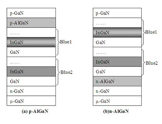
[0033] The substrate material of the existing GaN-based LED epitaxial wafer structure can be sapphire, SiC, Si, GaN, etc. The low-temperature buffer layer can be a low-temperature GaN layer or a low-temperature AlN layer, etc. When GaN is used as the substrate, the low-temperature buffer layer and the undoped GaN layer may not be grown. Multiple quantum well structures include InGaN / GaN structure, InGaN / AlGaN st...


PUM


Abstract

The invention discloses a GaN-base double-blue-light wavelength luminescent device and a preparation method thereof, aiming to solve the problem that the color rendering properties of a white-light LED (Light-emitting Diode) which is packaged by stimulating yellow-light fluorescent powder through a single-blue-light chip are not good. The structure of a GaN-base double-blue-light wavelength LED epitaxial wafer is sequentially composed of following members from a substrate: a GaN buffer layer, a GaN intrinsic layer, an n-GaN layer, an asymmetrical n-AlGaN layer, a high In component quantum well, a low In component quantum well and a p-GaN layer. The structure is characterized by leading the asymmetrical n-AlGaN layer between a mixed multi- quantum-well active layer and the n-GaN layer, removing a p-AlGaN electron barrier layer at the side of the p-GaN layer at the same time, and then packaging the double-blue-light wavelength chip and the yellow-light fluorescent powder to form the white-light LED.

Description

[0001] technical field [0002] The invention relates to the field of semiconductor optoelectronic devices, in particular to a GaN-based double blue wavelength light-emitting device and a preparation method thereof. Background technique [0003] Light-emitting diode is a semiconductor solid-state light source, which has many advantages such as small size, low energy consumption, low-voltage drive, fast response, long life, firm structure, strong shock and earthquake resistance, and environmental protection. It has very broad application prospects in lighting, display, indication, etc., so LED will become a new light source to replace traditional lighting devices in the 21st century. [0004] The preparation of GaN-based LED goes through three main steps: LED epitaxial wafer growth, LED chip preparation and LED packaging. There are many methods for growing GaN materials, such as: Metal Organic Chemical Vapor Phase Epitaxy (MOCVD), Molecular Beam Epitaxy (MBE), Halide Vapor P...

Claims


Application Information

Patent Timeline
Patent Type & Authority Applications(China)
IPC IPC(8): H01L33/14H01L33/00
Inventor 章勇严启荣李述体范广涵
Owner SOUTH CHINA NORMAL UNIVERSITY
Why Eureka
Try Eureka