
Tandem UV chamber for curing dielectric materials
a dielectric material and uv chamber technology, applied in drying machines, lighting and heating apparatus, furnaces, etc., can solve problems such as failure of dielectric materials during device operation, and achieve the effect of enhancing the uniformity of substrate illumination
- Summary
- Abstract
- Description
- Claims
- Application Information
AI Technical Summary
Benefits of technology
Problems solved by technology
Method used
Image

Examples
example 1
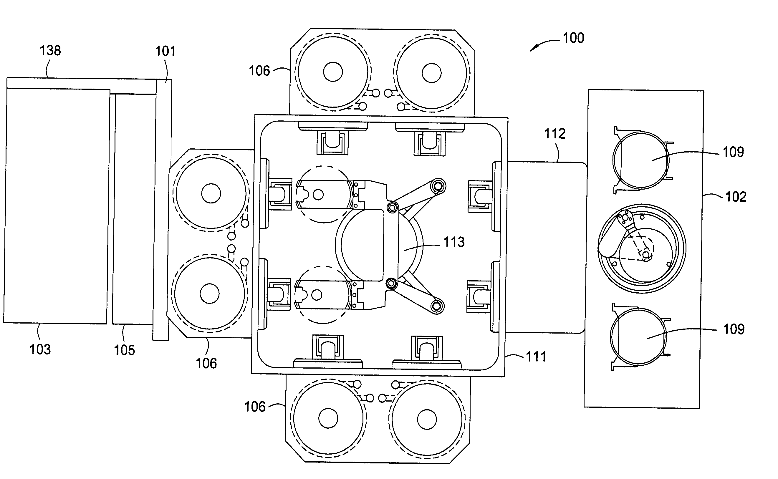
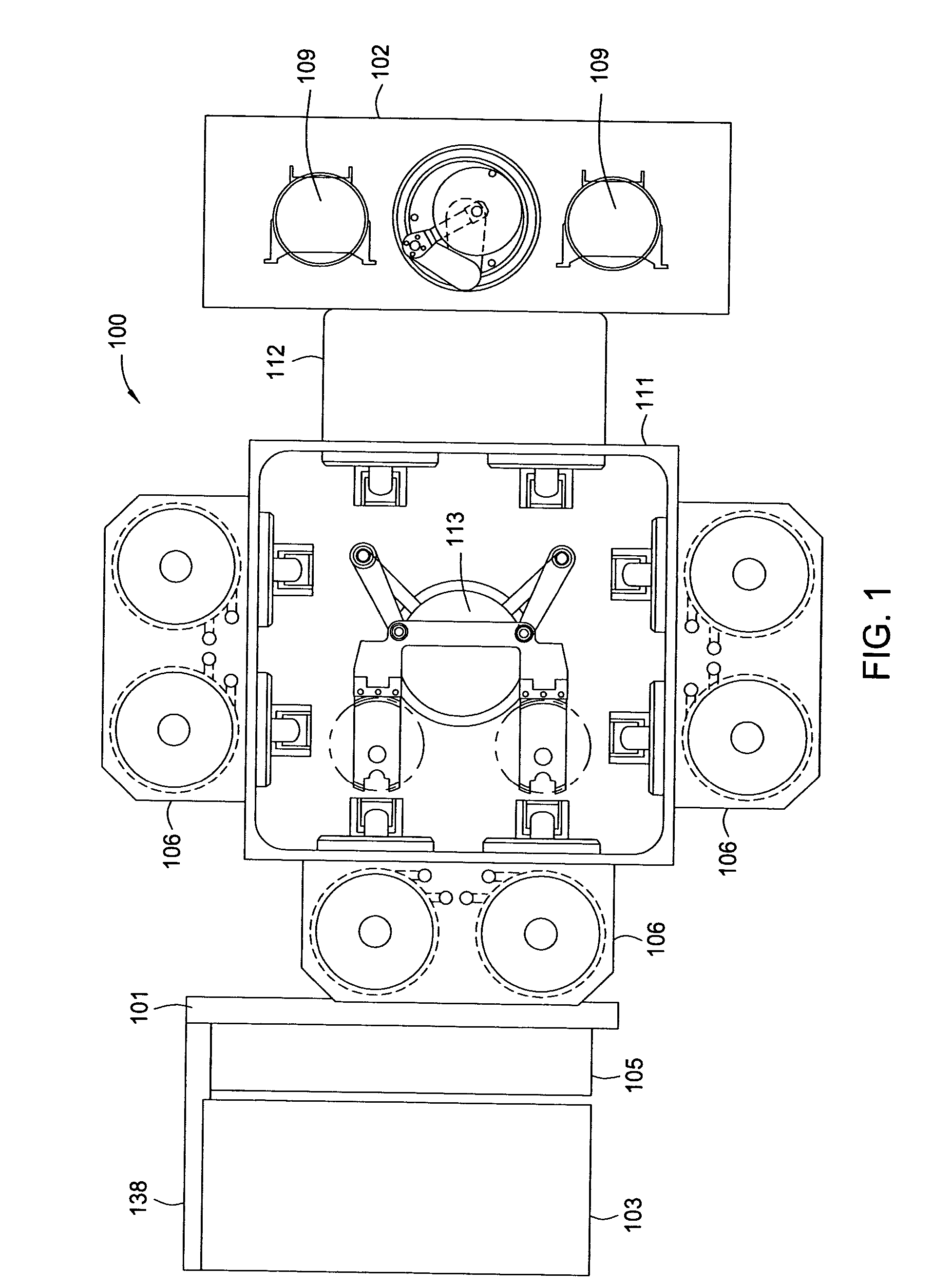
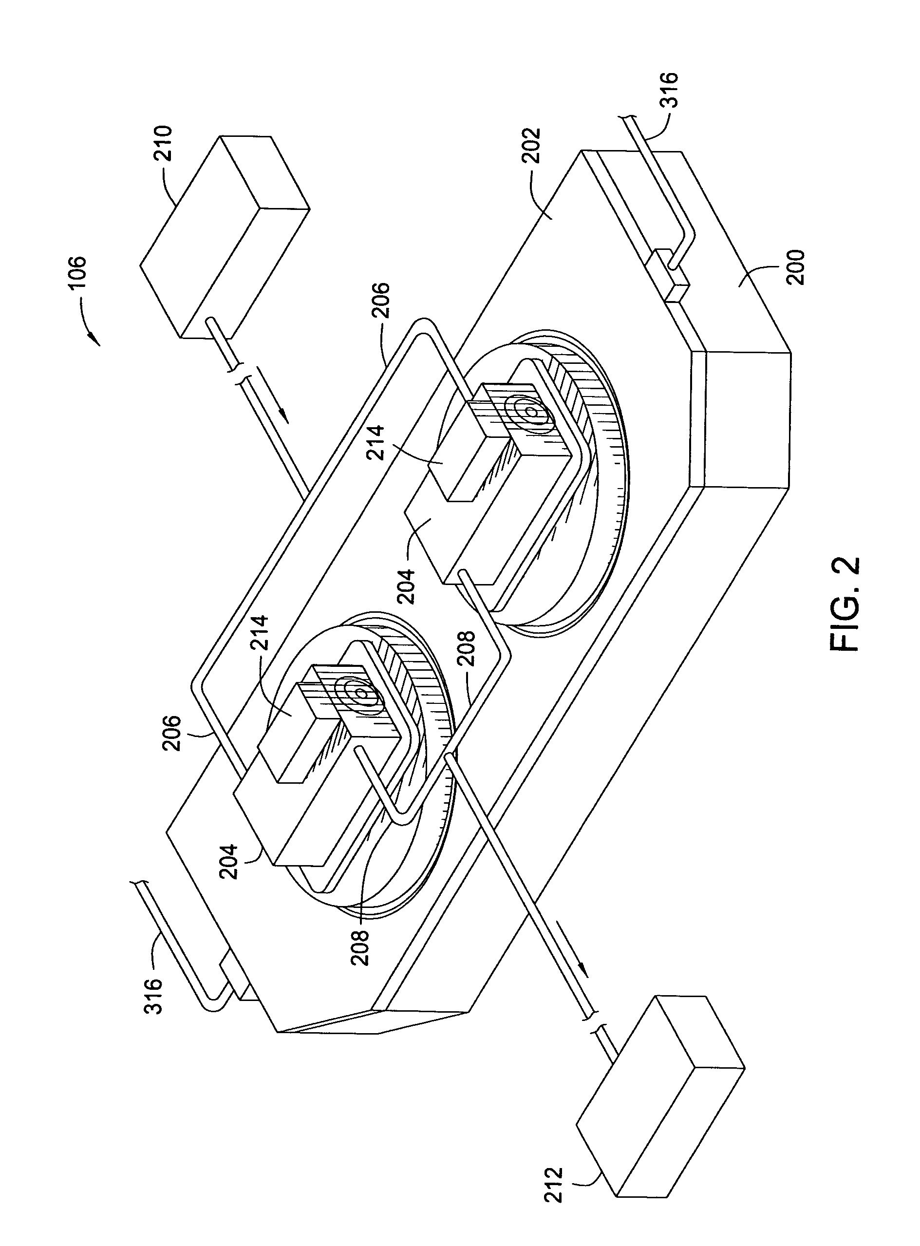
[0031] A cure process for a carbon doped silicon oxide film includes introduction of fourteen standard liters per minute (slm) of helium (He) at eight Torr for the tandem chamber 106 (7 slm per side of the twin) via each inlet passage 316. For some embodiments, the cure processes use nitrogen (N2) or argon (Ar) instead or as mixtures with He since primary concern is absence of oxygen unless other components are desired for reactive UV surface treatments. The purge gas essentially performs two main functions of removing curing byproducts and promoting uniform heat transfer across the substrate. These non-reactive purge gases minimize residue build up on the surfaces within the processing regions 300.
[0032] Additionally, hydrogen can be added to beneficially remove some methyl groups from films on the substrates 300 and also scavenge oxygen which is released during curing and tends to remove too many methyl groups. The hydrogen can getter residual oxygen remaining in the chamber afte...
example 2
[0036] For one embodiment, a clean process includes introduction of 5 slm of ozone and oxygen (13 wt % ozone in oxygen) into the tandem chamber, split evenly within each processing region 300 to generate sufficient oxygen radicals to clean deposits from surfaces within the processing regions 300. The O3 molecules can also attack various organic residues. The remaining O2 molecules do not remove the hydrocarbon deposits on the surfaces within the processing regions 300. A sufficient cleaning can occur with a twenty minute clean process at 8 Torr after curing six pairs of substrates.
[0037]FIG. 4 illustrates a partial section view of a lid assembly 402 with a UV bulb having a long axis 403 oriented vertically above a process region 400. The shape of the reflector in this embodiment is different than in any of the other embodiments. In other words, the reflector geometry must be optimized to ensure maximum intensity and uniformity of illumination of the substrate plane for each lamp sh...
PUM
 Abstract
Description
Claims
Application Information