Nonvolatile memory device having a plurality of trapping films

a technology of nonvolatile memory and trapping film, which is applied in the direction of semiconductor devices, basic electric elements, electrical appliances, etc., can solve the problems of difficult to improve or maintain the retention characteristics while improving both the programming and erasing efficiency of semiconductor devices incorporating a structure generally corresponding to the device illustrated in fig. 1, and achieves improved or comparable retention characteristics. , the effect of improving the erasing and programming efficiency

Inactive Publication Date: 2006-11-16
SAMSUNG ELECTRONICS CO LTD
View PDF3 Cites 27 Cited by
  • Summary
  • Abstract
  • Description
  • Claims
  • Application Information

AI Technical Summary

Benefits of technology

[0014] The invention provides nonvolatile memory devices and methods of producing such devices that exhibit improv...

Problems solved by technology

Accordingly, improving both the programming and erasing efficiency while improving or maintaining the retention characteristics...

Method used


Image

  • Nonvolatile memory device having a plurality of trapping films
  • Nonvolatile memory device having a plurality of trapping films
  • Nonvolatile memory device having a plurality of trapping films

Examples


Embodiment Construction

[0029] The invention will now be described more fully with reference to the accompanying drawings in which certain example embodiments of the invention are shown. As will be appreciated by those skilled in the art, however, the invention may be embodied in many different forms and should not be construed as being limited to the embodiments set forth herein. Indeed, these embodiments are provided so that this disclosure will be thorough and complete, and will fully convey the concept of the invention to those skilled in the art.

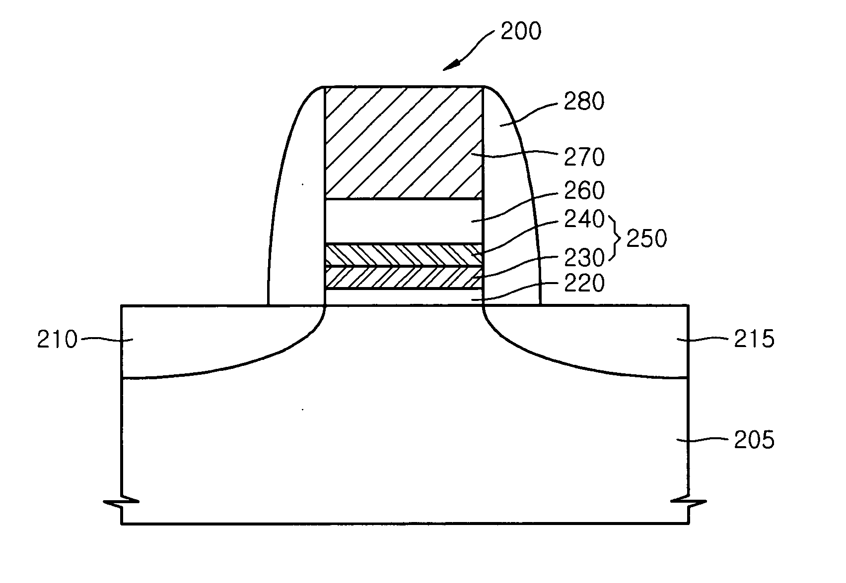
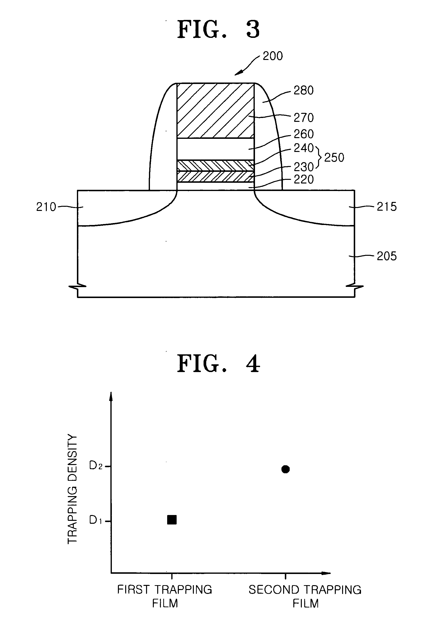
[0030]FIG. 3 is a cross-sectional view illustrating a nonvolatile memory device 200 according to an example embodiment of the invention. As illustrated in FIG. 3, the nonvolatile memory device 200 according to this example embodiment of the invention includes a tunneling insulating film 220, a storage node 250, a blocking insulating film 260, and a control gate electrode 270 formed on a semiconductor substrate 205 between source and drain regions 210, 215. Mo...


PUM


Abstract

Provided is a nonvolatile memory device which includes a tunneling insulating film formed on a semiconductor substrate, a storage node formed on the tunneling insulating film, a blocking insulating film formed on the storage node, and a control gate electrode formed on the blocking insulating film. The storage node includes at least two trapping films having different trap densities, and the blocking insulating film has a dielectric constant greater than that of the silicon oxide film.

Description

PRIORITY STATEMENT [0001] This application claims the benefit of Korean Patent Application No. 10-2005-0012914, filed on Feb. 16, 2005, in the Korean Intellectual Property Office, the disclosure of which is incorporated herein, in its entirety, by reference. BACKGROUND OF THE INVENTION [0002] 1. Field of the Invention [0003] The invention is directed to nonvolatile memory devices and methods of fabricating such devices, and more particularly, to nonvolatile memory devices that incorporate a storage node for storing charges and methods of manufacturing memory devices including such storage nodes. [0004] 2. Description of the Related Art [0005] During the writing and erasing of data, nonvolatile memory devices may utilize one or more methods including, for example, modifying a threshold voltage transition of a transistor, displacing charge and / or changing a resistance. Those nonvolatile memory devices that utilize the method of modifying a threshold voltage transition typically includ...

Claims


Application Information

Patent Timeline
IPC IPC(8): H01L29/792
CPCH01L29/4232H01L29/42324H01L29/792H01L29/7881H01L29/513
Inventor KIM, JU-HYUNGHAN, JEONG-HEEKIM, CHUNG-WOOMIN, YO-SEPKIM, MOON-KYUNGJEONG, YOUN-SEOK
Owner SAMSUNG ELECTRONICS CO LTD
Why Eureka
Try Eureka