CMOS devices for low power integrated circuits

a low-power integrated circuit and circuit technology, applied in the field of semiconductor devices, can solve the problems of limited application to dram devices, does not address the low leakage-power requirements, and the engineering of asymmetric devices is not specially tailored, so as to reduce the off-state leakage current

Inactive Publication Date: 2006-12-07
TAIWAN SEMICON MFG CO LTD
View PDF18 Cites 35 Cited by
  • Summary
  • Abstract
  • Description
  • Claims
  • Application Information

AI Technical Summary

Benefits of technology

[0005] These and other problems are generally solved or circumvented, and technical advantages are generally achieved by preferred embod

Problems solved by technology

The more abrupt and low-resistance junctions increase the device off-state leakage current and power thus creating a barrier for the continued scaling of CMOS devices for low standby power ICs used in mobile and other application segments.
However, this approach is limited

Method used


Image

  • CMOS devices for low power integrated circuits
  • CMOS devices for low power integrated circuits
  • CMOS devices for low power integrated circuits

Examples


Embodiment Construction

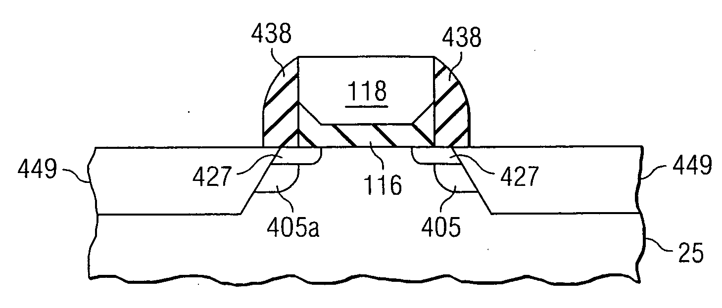
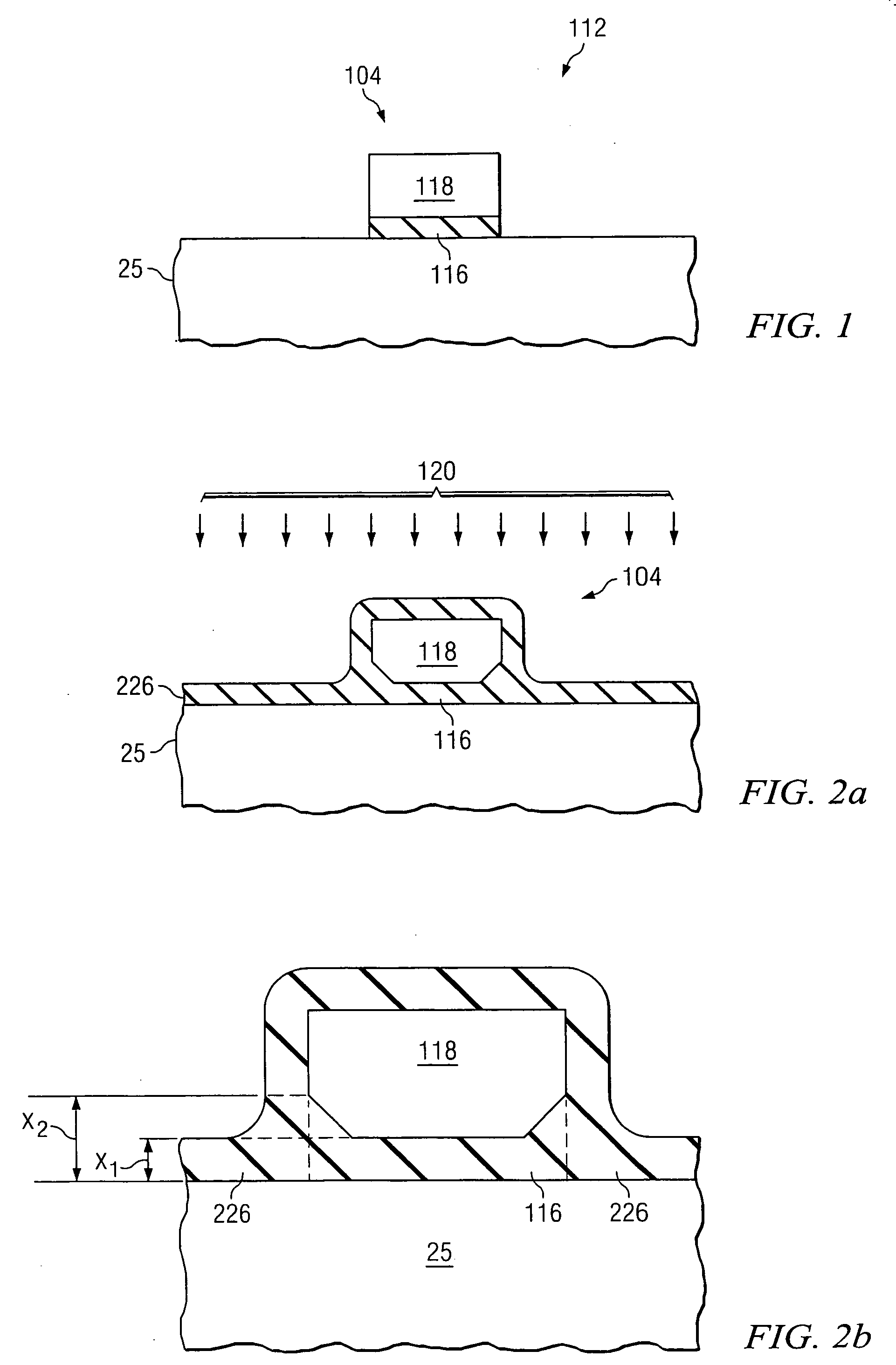
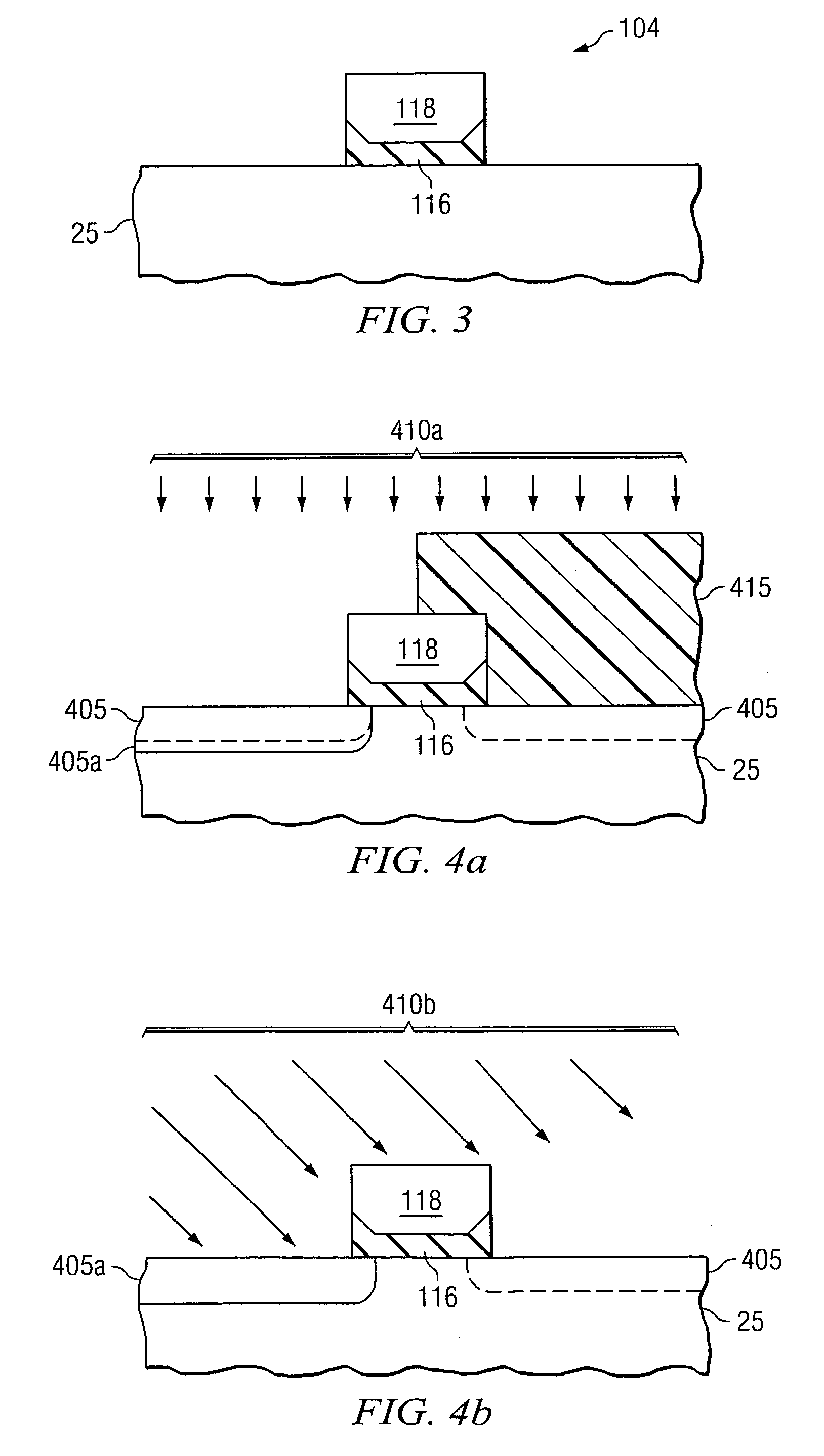
[0019] The making and using of the presently preferred embodiments are discussed in detail below. It should be appreciated, however, that the present invention provides many applicable inventive concepts that can be embodied in a wide variety of specific contexts. The specific embodiments discussed are merely illustrative of specific ways to make and use the invention, and do not limit the scope of the invention. The intermediate stages of manufacturing a preferred embodiment of the present invention are illustrated throughout the various views and illustrative embodiments of the present invention. To more clearly illustrate certain embodiments, a letter indicating variations of the same structure, material, or process step may follow a figure number.

[0020] This invention relates generally to semiconductor device fabrication and more particularly to structures and methods for devices formed on semiconductor substrates. The present invention will now be described with respect to pre...


PUM


Abstract

A preferred embodiment of the invention provides a semiconductor fabrication method. An embodiment comprises forming a MOS device and thermally oxidizing the MOS device to form a gate dielectric substantially thicker at a gate dielectric edge than that at a gate dielectric center. Embodiments further comprise performing a source/drain ion implant to form an asymmetric source/drain, wherein the source region includes a high leakage source junction, and wherein the drain region includes a low leakage drain junction. Other embodiments of the invention comprise a MOS device formed in a semiconductor substrate, wherein the device has improved resistance to floating body effects. Still other embodiments include a CMOS device for low power integrated circuits.

Description

TECHNICAL FIELD [0001] This invention relates generally to semiconductor devices, and, more particularly, to integrated circuits and to methods for controlling off-state leakage currents. BACKGROUND [0002] The need for overall performance and power improvements as well as the integration density drives the CMOS device size reduction. This in turn places a fundamental requirement on the depth, abruptness, and resistance of the drain and source junctions in NMOS and PMOS devices. The more abrupt and low-resistance junctions increase the device off-state leakage current and power thus creating a barrier for the continued scaling of CMOS devices for low standby power ICs used in mobile and other application segments. [0003] One approach to improve DRAM data retention time is by forming pass transistors with asymmetric source and drain structures as reported by Shito et al., in U.S. Pat. No. 6,238,967. However, this approach is limited to DRAM applications and does not address the low le...

Claims


Application Information

Patent Timeline
IPC IPC(8): H01L29/76
CPCH01L21/26586H01L21/28247H01L29/66659H01L29/42368H01L29/6659H01L29/1083H01L29/7833
Inventor DIAZ, CARLOS H.CHANG, MI-CHANG
Owner TAIWAN SEMICON MFG CO LTD
Why Eureka
Try Eureka