Array substrate, method for producing the same and display device

a technology of array substrate and substrate, which is applied in the direction of semiconductor devices, electrical devices, transistors, etc., can solve the problems of affecting the normal use of tft, the resistance of tft in normal operation is too large, and the crystalline characteristics of polysilicon tft cannot be effectively recovered, so as to reduce the off-state leakage current ion, reduce the on-state current ion, and reduce the off-state leakage current io

Inactive Publication Date: 2016-12-15
BOE TECH GRP CO LTD
View PDF5 Cites 6 Cited by
  • Summary
  • Abstract
  • Description
  • Claims
  • Application Information

AI Technical Summary

Benefits of technology

[0008]In view of this, embodiments of the present disclosure are intended to provide an array substrate, a method for producing the same and a display device including the same, so as to overcome the defect present in the art that when the TFT is working, an ON-state current is reduced due to the presence of the LDD structure provided for reducing the TFT's Off-state current.
[0036]The array substrate of the present disclosure is provided with the first gate 3 (bottom gate) and the second gate 7 (top gate) and employs the LDD structure. On one hand, in combination with a working principle of the bottom gate structure, when the TFT is working (i.e., the top gate is applied with a gate voltage), the bottom gate is also switched on to cause the LDD region to induce carriers; in this way, the LDD region under the action of an electric field of the bottom gate and with the carriers being generated at the lightly doped regions can avoid the disadvantageous effect of reducing the On-state current Ion caused by the lightly doping. On the other hand, when the electric field of the top gate of the TFT is removed, the bottom gate is switched off, and meanwhile the electric field of the bottom gate is also removed, thereby reducing the Off-state leakage current of the TFT. That is, the advantage that the LDD structure can reduce the Off-state leakage current Ioff is utilized.

Problems solved by technology

Due to thermodynamic limitation of the glass, crystalline characteristics of the poly-silicon TFT cannot be effectively recovered by annealing after ion implantation.
A relatively large leakage current occurring in the presence of a reversed bias voltage, will affect normal use of the TFT.
Due to the provision of the LDD region, when the TFT is in a normal operation, ON-state current is often affected, which causes the TFT in the normal operation to have too large resistance and cause increasing of a power dissipation thereof.

Method used


Image

  • Array substrate, method for producing the same and display device
  • Array substrate, method for producing the same and display device
  • Array substrate, method for producing the same and display device

Examples


Embodiment Construction

[0040]The specific embodiments of the present disclosure are described in detail in conjunction with the drawings and examples thereof. The following embodiments are intended to explain the present disclosure, rather than limiting the scope of the present disclosure.

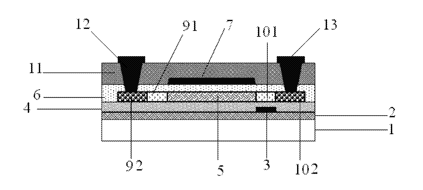
[0041]As shown in FIG. 6, an array substrate 100 provided in accordance with one or more of embodiments of the present disclosure includes a substrate 1, a buffer layer 2 (optionally) provided onto the substrate 1, a first gate (i.e., a bottom gate) 3 and a first gate insulation layer 4. An active layer 5 is provided onto the first gate insulation layer 4, and a second gate insulation layer 6, a second gate (i.e., a top gate) 7, a third gate insulation layer 11, a source electrode 12 and a drain electrode 13 are arranged on the active layer 5 in sequence, and the source electrode 12 and the drain electrode 13 are located on the third gate insulation layer 11. Two side regions of the active layer 5 outside a region thereo...


PUM


Abstract

Disclosed are an array substrate, a method for producing the same and a display device including the same. The array substrate includes a substrate; a first gate, a first gate insulation layer, an active layer, a second gate insulation layer, a second gate, a third gate insulation layer and source and drain electrodes provided on the substrate in sequence. Two side regions outside a region of the active layer corresponding to the second gate are source and drain-lightly doped regions and source and drain-heavily doped regions, respectively. The source and drain electrodes are contacted with the heavily doped source and drain regions, respectively. The first gate is provided below the lightly doped drain region corresponding to the drain electrode, or the first gate includes first and second sub parts which are respectively provided below the lightly doped source and drain regions corresponding to the source and drain electrodes respectively.

Description

CROSS-REFERENCE TO RELATED APPLICATION[0001]This application claims the benefit of Chinese Patent Application No. 201410806984.2 filed on Dec. 22, 2014 and entitled as “Display device, Array Substrate and Method for Producing The Same” in the State Intellectual Property Office of China, the whole disclosure of which is incorporated herein by reference.BACKGROUND OF THE INVENTION[0002]Field of the Invention[0003]The present disclosure relates to the technical field of display process, and particularly, to an array substrate, a method for producing the same and a display device including the array substrate.[0004]Description of the Related Art[0005]In Liquid Crystal Displays (LCDs) or Organic Light-Emitting Displays (OLEDs), each pixel point is driven by a Thin Film Transistor (TFT) integrated behind the pixel point, thereby displaying screen information with high speed, high brightness and high contrast. In the prior art, it is often to manufacture the TFT by poly-silicon or amorphou...

Claims


Application Information

Patent Timeline
Patent Type & Authority Applications(United States)
IPC IPC(8): H01L29/786H01L29/66H01L21/426H01L21/027H01L21/266H01L27/12H01L21/02
CPCH01L29/78648H01L21/426H01L29/7869H01L27/1225H01L27/1222H01L29/78672H01L29/78603H01L27/1218H01L29/66969H01L29/6675H01L27/1274H01L21/02565H01L21/02532H01L21/02592H01L21/02595H01L21/02675H01L21/0273H01L21/266H01L29/78618H01L27/1214H01L29/0847H01L29/401H01L29/42384H01L29/66484H01L29/66492H01L21/28H01L29/78645H01L29/786
Inventor SHI, LEIXU, XIAOWEI
Owner BOE TECH GRP CO LTD
Why Eureka
Try Eureka