Three-dimensional integrated circuit structure and method of making same

a technology of integrated circuits and manufacturing methods, applied in the direction of transistors, solid-state devices, nanoinformatics, etc., can solve problems such as wide us

Inactive Publication Date: 2006-12-07
BESANG
View PDF23 Cites 301 Cited by
  • Summary
  • Abstract
  • Description
  • Claims
  • Application Information

AI Technical Summary

Problems solved by technology

However, both the laser recrystallization and the epitaxial processes described above are have drawbacks, such as requiring high temperature operations, which are incompatible with the low temperature processing required for many semiconductor devices; and further, single crystalline semiconductor layers formed in this way may have many defects, and therefore these methods are not widely used.

Method used


Image

  • Three-dimensional integrated circuit structure and method of making same
  • Three-dimensional integrated circuit structure and method of making same
  • Three-dimensional integrated circuit structure and method of making same

Examples


Embodiment Construction

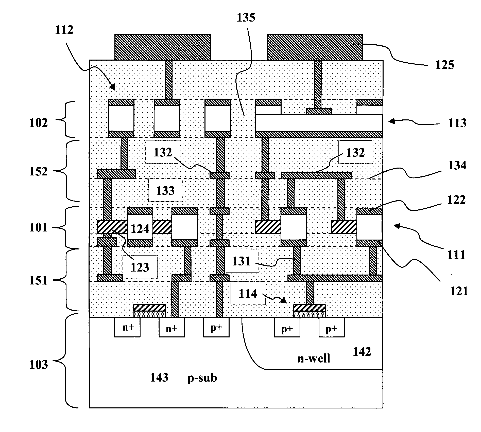
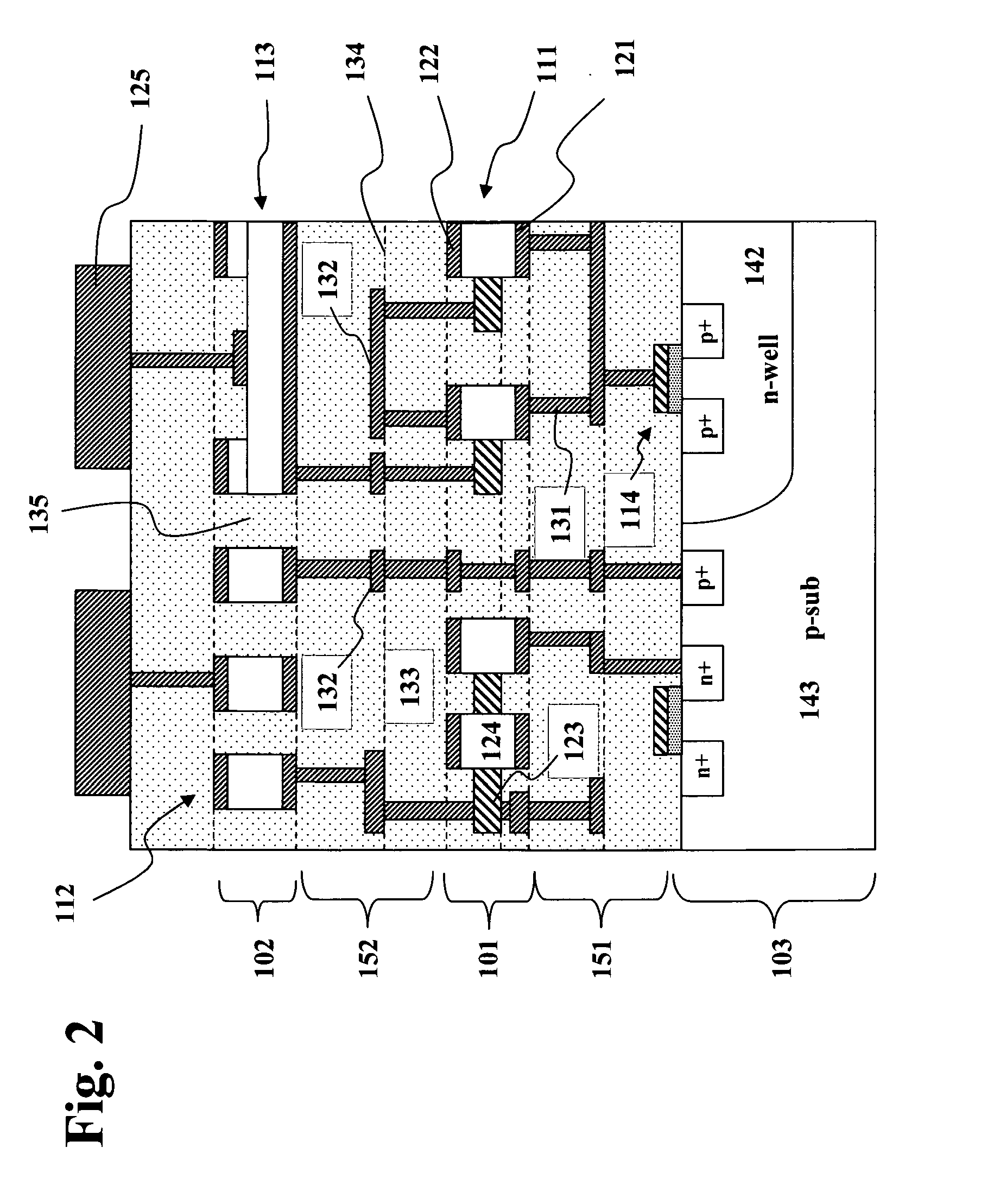
[0065] A 3-D IC in accordance with the present invention is shown in FIG. 2. Embodiments of the present invention provide a device integration technology.

[0066] Reference herein to “one embodiment”, “an embodiment”, or similar formulations, means that a particular feature, structure, operation, or characteristic described in connection with the embodiment, is included in at least one embodiment of the present invention. Thus, the appearances of such phrases or formulations herein are not necessarily all referring to the same embodiment. Furthermore, various particular features, structures, operations, or characteristics may be combined in any suitable manner in one or more embodiments.

Terminology

[0067]“ASIC” refers to Application Specific Integrated Circuit. “SoC” refers to a System on a Chip, with “SoCs” being the plural of SoC. A SoC may be an ASIC but is not required to be. An ASIC may be a SoC but is not required to be.

[0068] The expression “back bias”, as used herein, refe...


PUM

PropertyMeasurementUnit
temperatureaaaaaaaaaa
temperaturesaaaaaaaaaa
melting pointsaaaaaaaaaa

Abstract

Vertically oriented semiconductor devices may be added to a separately fabricated substrate that includes electrical devices and / or interconnect. The plurality of vertically oriented semiconductor devices are physically separated from each other, and are not disposed within the same semiconductor body, or semiconductor substrate. The plurality of vertically oriented semiconductor devices may be added to the separately fabricated substrate as a thin layer including several doped semiconductor regions which, subsequent to attachment, are etched to produce individual doped stack structures. Alternatively, the plurality of vertically oriented semiconductor devices may be fabricated prior to attachment to the separately fabricated substrate. The doped stack structures may form the basis for diodes, capacitors, n-MOSFETs, p-MOSFETs, bipolar transistors, and floating gate transistors. Ferroelectric memory devices, Ferromagnetic memory devices, chalcogenide phase change devices, may be formed in a stackable add-on layer for use in conjunction with a separately fabricated substrate. Stackable add-on layers may include interconnect lines.

Description

FIELD OF THE INVENTION [0001] The present invention relates generally to three dimensional integrated circuit (IC) structures and manufacturing methods therefore, and more particularly relates to combining a semiconductor substrate with a thin add-on semiconductor layer in which various active and / or passive devices have been fabricated. [0002] As shown in FIG. 1, a prior art 3-D IC might be termed a ‘Hybrid IC’. A conventional Hybrid IC implementation method typically includes; providing a first IC which consists of a base semiconductor substrate 201 and a dielectric layer 202; providing a second IC that also consists of a base semiconductor substrate 203 and a dielectric layer 204; stacking and bonding these ICs, or individual chips; and implementing a deep via 255 such as shown in U.S. Pat. No. 6,600,173 which penetrates the semiconductor substrate, or providing micro bumps as shown in U.S. Pat. No. 6,355,501. [0003] Still referring to FIG. 1, it is noted that devices in the stac...

Claims


Application Information

Patent Timeline
Patent Type & Authority Applications(United States)
IPC IPC(8): H01L21/84H01LH01L21/30H01L21/301H01L21/46H01L27/06H01L31/072
CPCB82Y10/00H01L27/2454H01L21/84H01L27/0688H01L27/10805H01L27/11H01L27/1104H01L27/112H01L27/11206H01L27/115H01L27/11502H01L27/11507H01L27/11556H01L27/11568H01L27/228H01L28/55H01L29/78642H01L29/7881H01L29/792H01L29/7926H01L29/8613H01L29/872H01L21/8221H10B63/34H10B61/22H10B12/30H10B10/00H10B10/12H10B20/00H10B20/20H10B53/30H10B53/00H10B41/27H10B43/30H10B69/00
Inventor LEE, SANG-YUN
Owner BESANG
Why Eureka
Try Eureka