Microelectromechanical device array and method for driving the same

a micro-electromechanical and array technology, applied in static indicating devices, instruments, optics, etc., can solve the problems of difficult to tilt the movable mirror, the micro-electromechanical device array has difficulty in operating at high speed, and the light reflection cannot be performed in the left-tilting state, etc., to achieve the effect of high speed

Inactive Publication Date: 2006-12-14
FUJIFILM CORP +1
View PDF1 Cites 28 Cited by
  • Summary
  • Abstract
  • Description
  • Claims
  • Application Information

AI Technical Summary

Benefits of technology

[0032] According to an aspect of the invention, address rewriting can be performed without malfunction even while the movable mirror is vibrating. Therefore, a microelectromechanical device array capable of operating at high speed can be provided.

Problems solved by technology

However, it is difficult to tilt the movable mirror, which has been already tilted, in an opposite direction, and hence a conventional method has been employed in which the movable mirror is controllably driven while performing complex voltage control.
As a result, light reflection cannot be performed in the left-tilted state, and this will cause a malfunction.
Therefore, according to the conventional method, next-address rewriting (zone A) is performed after waiting for the end of zone E (in the example illustrated in FIG. 5, after a lapse of 22 μs), and hence the microelectromechanical device array has difficulty in operating at high speed.
However, there is no conventional technique for ensuring the address rewriting without malfunction.

Method used


Image

  • Microelectromechanical device array and method for driving the same
  • Microelectromechanical device array and method for driving the same
  • Microelectromechanical device array and method for driving the same

Examples


first embodiment

(First Embodiment)

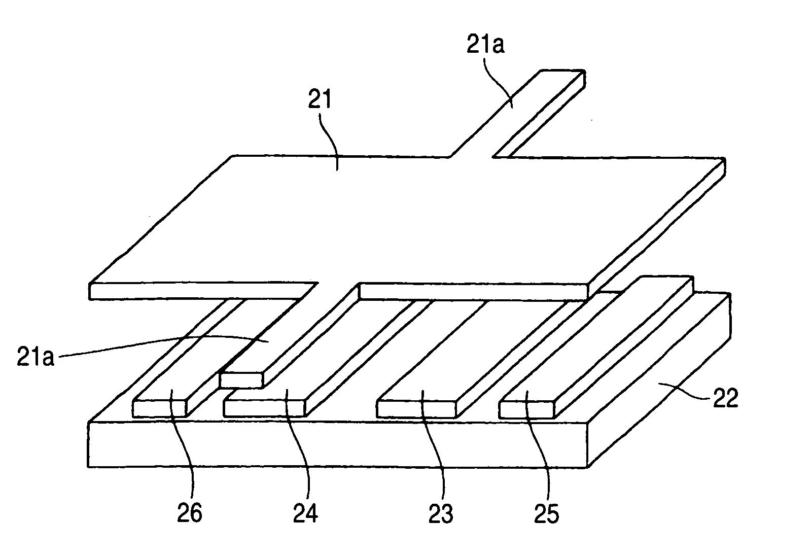
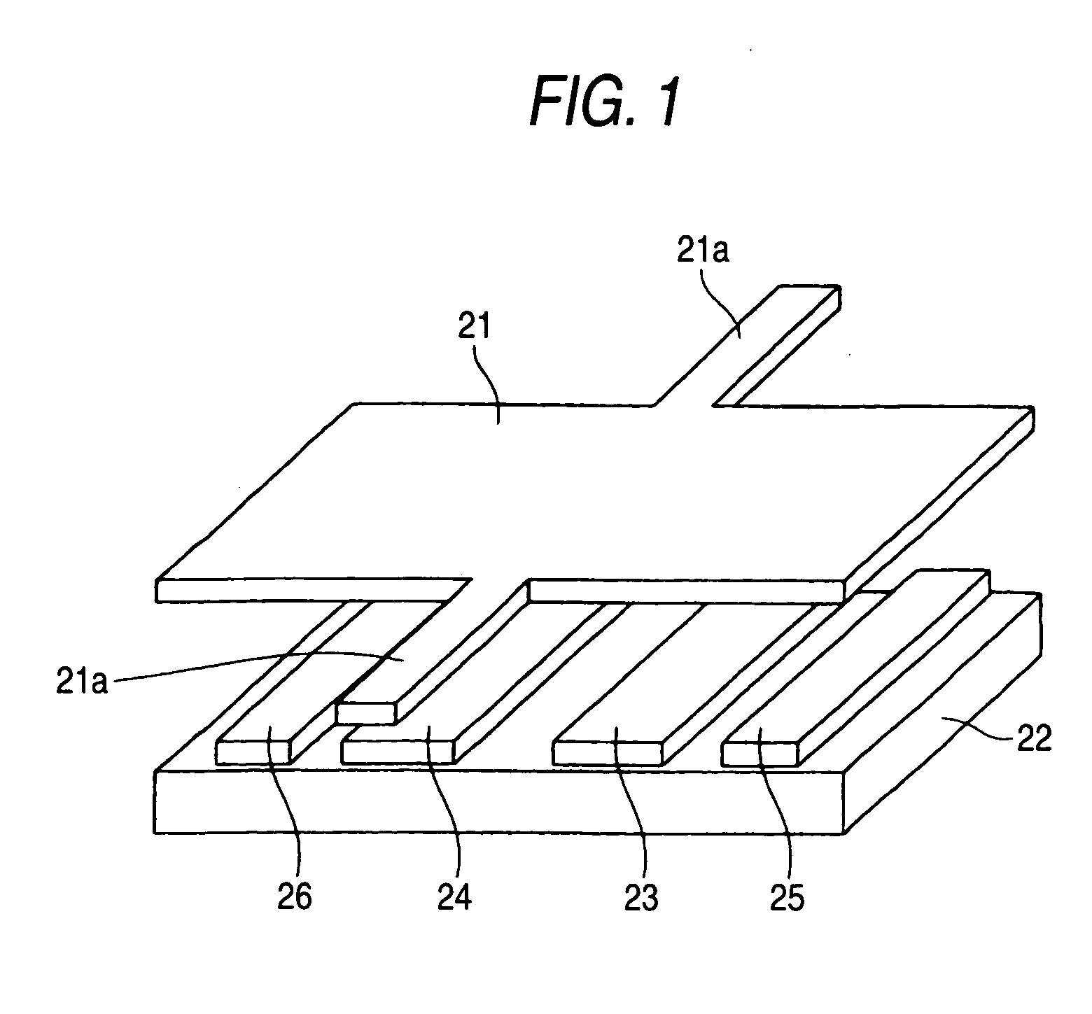
[0040]FIG. 1 is a schematic drawing that illustrates one microelectromechanical device drawn from among an array of microelectromechanical devices that constitute a microelectromechanical device array according to a first embodiment of the present invention. movable portion (hereinafter referred to as a “movable mirror”) 21 of the microelectromechanical device array in this embodiment is supported in a space by extending a hinge 21a between two supporting rods (not shown) formed on the surface of a semiconductor substrate 22, so that the movable mirror 21 can swing. Fixed electrode films (hereinafter referred to as a “Fixed electrode films”) 23 and 24 are formed on the surface of the semiconductor substrate 22 facing the back surface of the movable mirror 21.

[0041] As illustrated in FIG. 1, the fixed electrode film 23 is formed at the position facing the right part of the back surface of the movable mirror 21 with respect to the hinge 21a thereof, whereas the fixe...

second embodiment

(Second Embodiment)

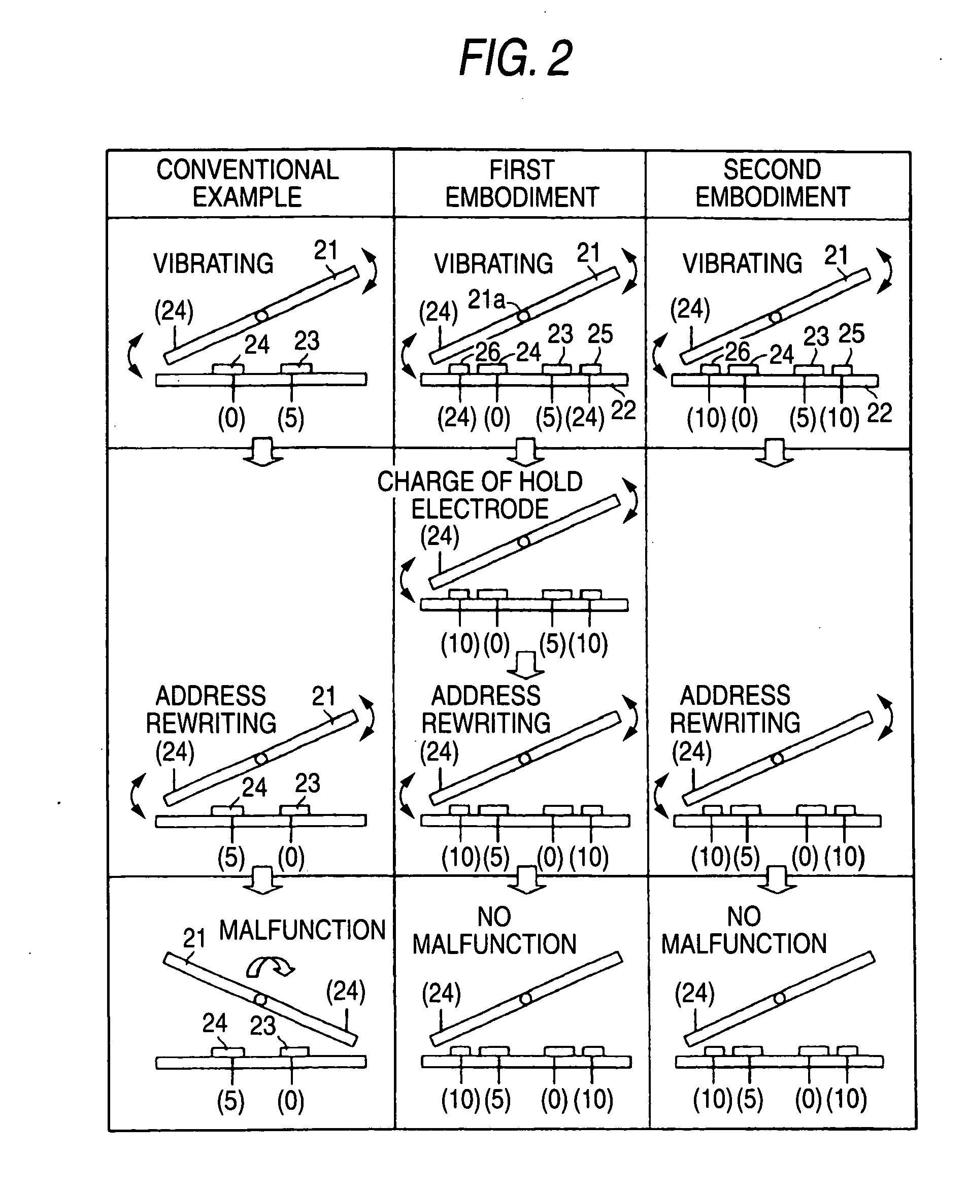
[0055] The right column in FIG. 2 illustrates a method for driving a microelectromechanical device array according to a second embodiment of the invention. In the first embodiment mentioned above, the bias voltage Vb is 24V when the process reaches zone E. At this time, the same voltage of 24V as the bias voltage Vb is applied to the hold electrode films 25 and 26. Thereafter, the hold voltage to be applied to the hold electrode films 25 and 26 is reduced to 10V before performing address rewriting (i.e., the rewriting of the voltage Va).

[0056] On the other hand, in this embodiment, a hold voltage of 10V is always applied to the hold electrode films 25 and 26 without changing the hold voltage to be applied to the hold electrode films 25 and 26. According to this method, there is no fear that the movable mirror 21 will cause a malfunction even when address rewriting is performed while the movable mirror 21 is vibrating as in the first embodiment.

[0057] In each emb...


PUM


Abstract

In a microelectromechanical device array including an array of devices arranged at least one of one-dimensionally and two-dimensionally each of which includes a movable portion that is supported to be elastically deformed and that has a movable electrode on at least one part thereof and fixed electrodes that are disposed to face the movable portion and by which the movable portion is moved to one of at least two different positions, hold electrodes are disposed beside the fixed electrodes, and a hold voltage is applied to the hold electrodes and before rewriting an address voltage that is applied to the fixed electrodes so as to fix the position state of the movable portion.

Description

BACKGROUND OF THE INVENTION [0001] 1. Field of the Invention [0002] The invention relates to a microelectromechanical device array and a method for driving the microelectromechanical device array at a high speed. [0003] 2. Background Art [0004] JP-A-10-48543 (the term “JP-A” as used herein means an “unexamined published Japanese patent application) discloses a conventional method for driving a microelectromechanical device array, such as a DMD (Digital Micro-mirror Device). This conventional driving method will be described with reference to FIGS. 3 to 5. [0005]FIG. 3 is a schematic drawing that illustrating two of an array of microelectromechanical devices that constitute a microelectromechanical device array. A semiconductor substrate 1 contains a drive circuit, not shown, therein, and has movable mirrors 2 and 3 disposed on the surface thereof. [0006] Each of the movable mirrors 2 and 3 is supported in a space by a hinge 6 extended between supporting rods 4 and 5 erected on the s...

Claims


Application Information

Patent Timeline
Patent Type & Authority Applications(United States)
IPC IPC(8): G09G3/34
CPCG09G2300/0426G09G3/346
Inventor OGIKUBO, SHINYANAKAMURA, HIROCHIKA
Owner FUJIFILM CORP
Why Eureka
Try Eureka