
Non-volatile memory device having floating gate and methods forming the same

a non-volatile memory and gate technology, applied in the direction of semiconductor devices, electrical devices, transistors, etc., can solve the problems of operating voltage dropping, difficult to increase the capacitance between the control gate electrode and the floating gate, and the mask rom non-volatile memory devi

Inactive Publication Date: 2006-12-21
SAMSUNG ELECTRONICS CO LTD
View PDF2 Cites 80 Cited by
  • Summary
  • Abstract
  • Description
  • Claims
  • Application Information

AI Technical Summary

Problems solved by technology

Non-volatile memory devices may retain their stored data even when their power supplies are interrupted.
However, there are certain difficulties associated with mask ROM non-volatile memory devices in connection with their ability to erase and program data which has already been written.
In addition, as the operating voltage is inversely proportional to the coupling ratio, increasing the coupling ratio may result in the operating voltage dropping as well.
However, there may be difficulties associated with the above-mentioned conventional method when seeking to form a highly integrated semiconductor device because within a limited area, it may be difficult to increase the capacitance between a control gate electrode and a floating gate.

Method used


Image

  • Non-volatile memory device having floating gate and methods forming the same
  • Non-volatile memory device having floating gate and methods forming the same
  • Non-volatile memory device having floating gate and methods forming the same

Examples


Embodiment Construction

[0018] The Exemplary Embodiments of the present invention will be described more fully hereinafter with reference to the accompanying drawings. This invention, however, may be embodied in many different forms and should not be construed as limited to the embodiments set forth herein.

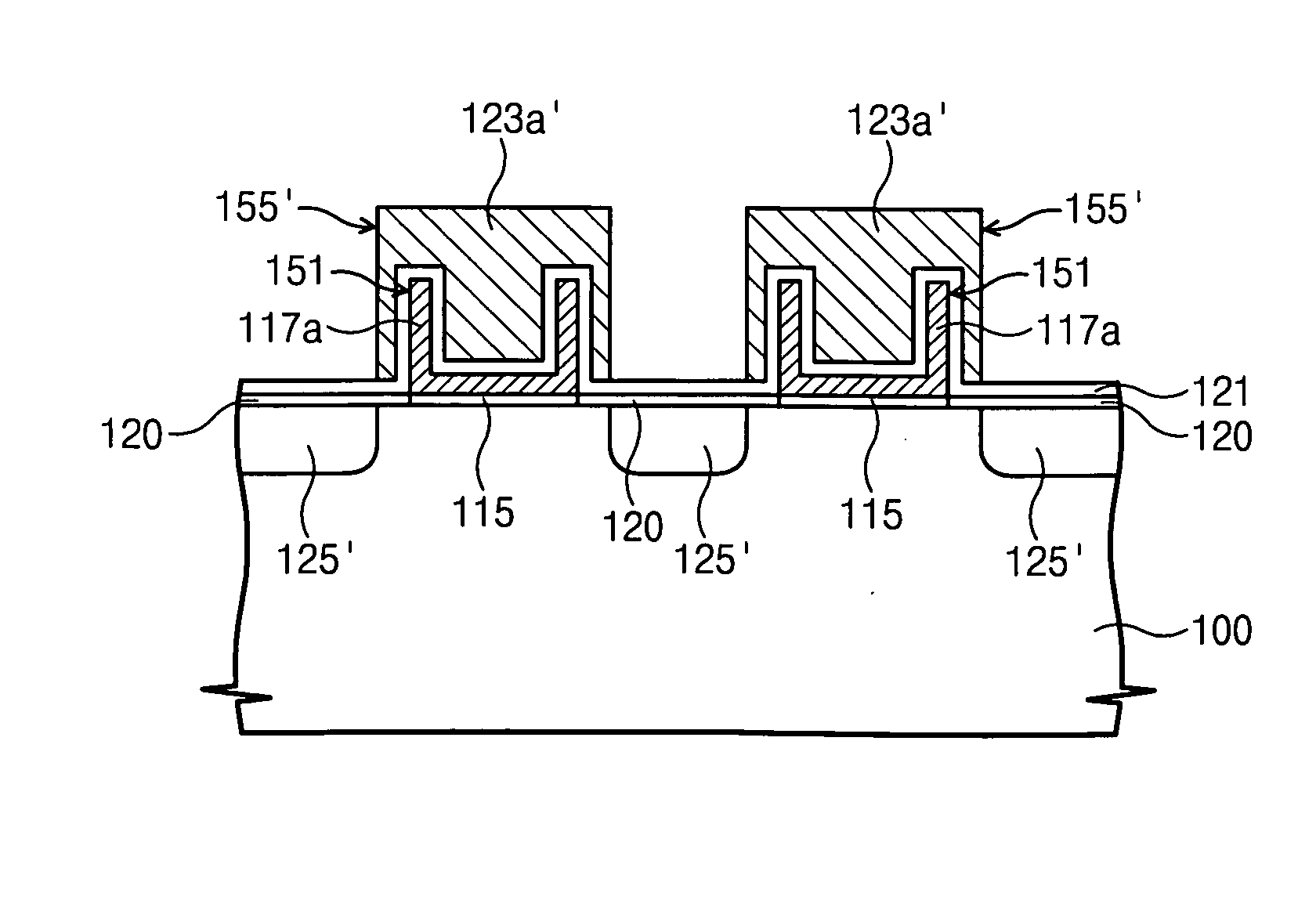
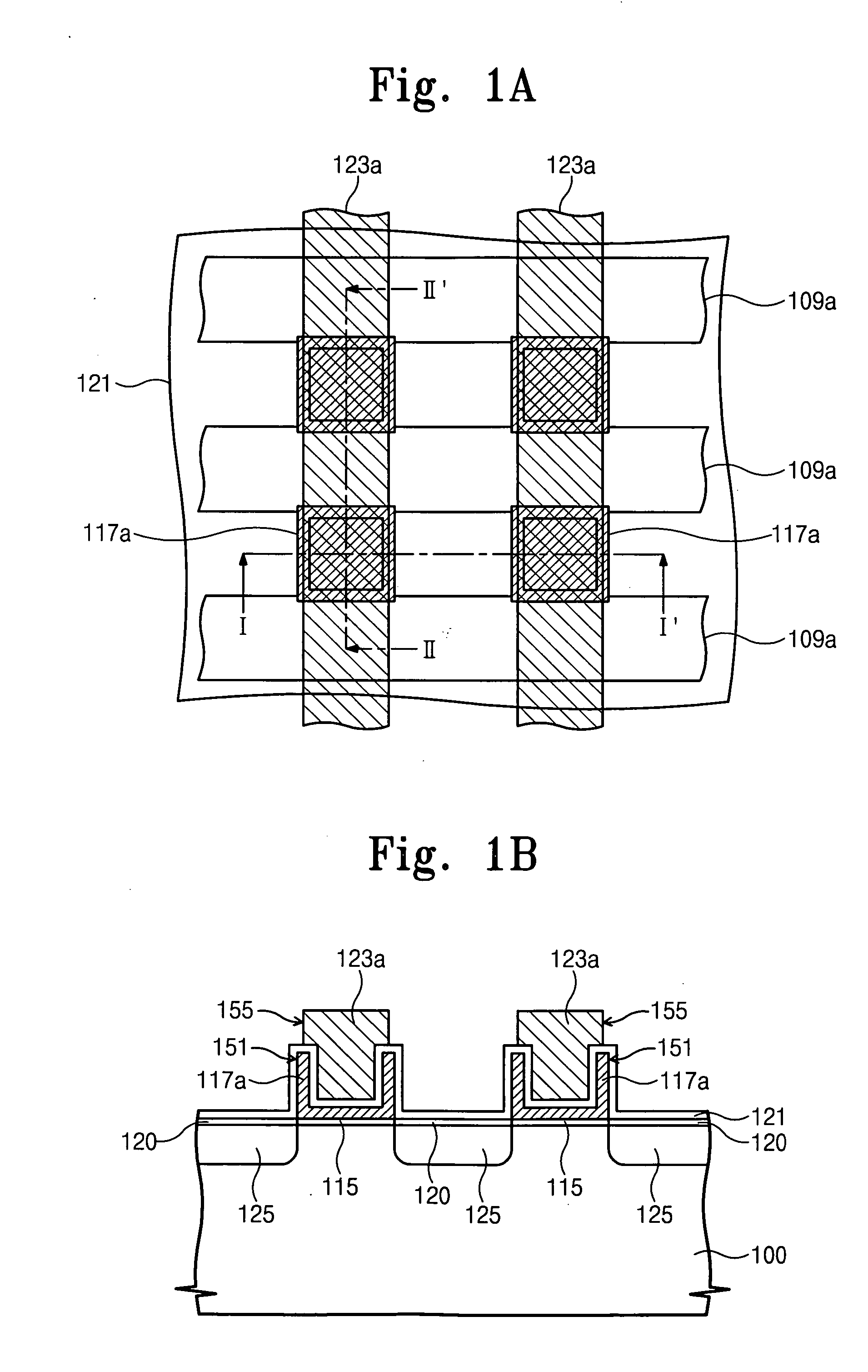
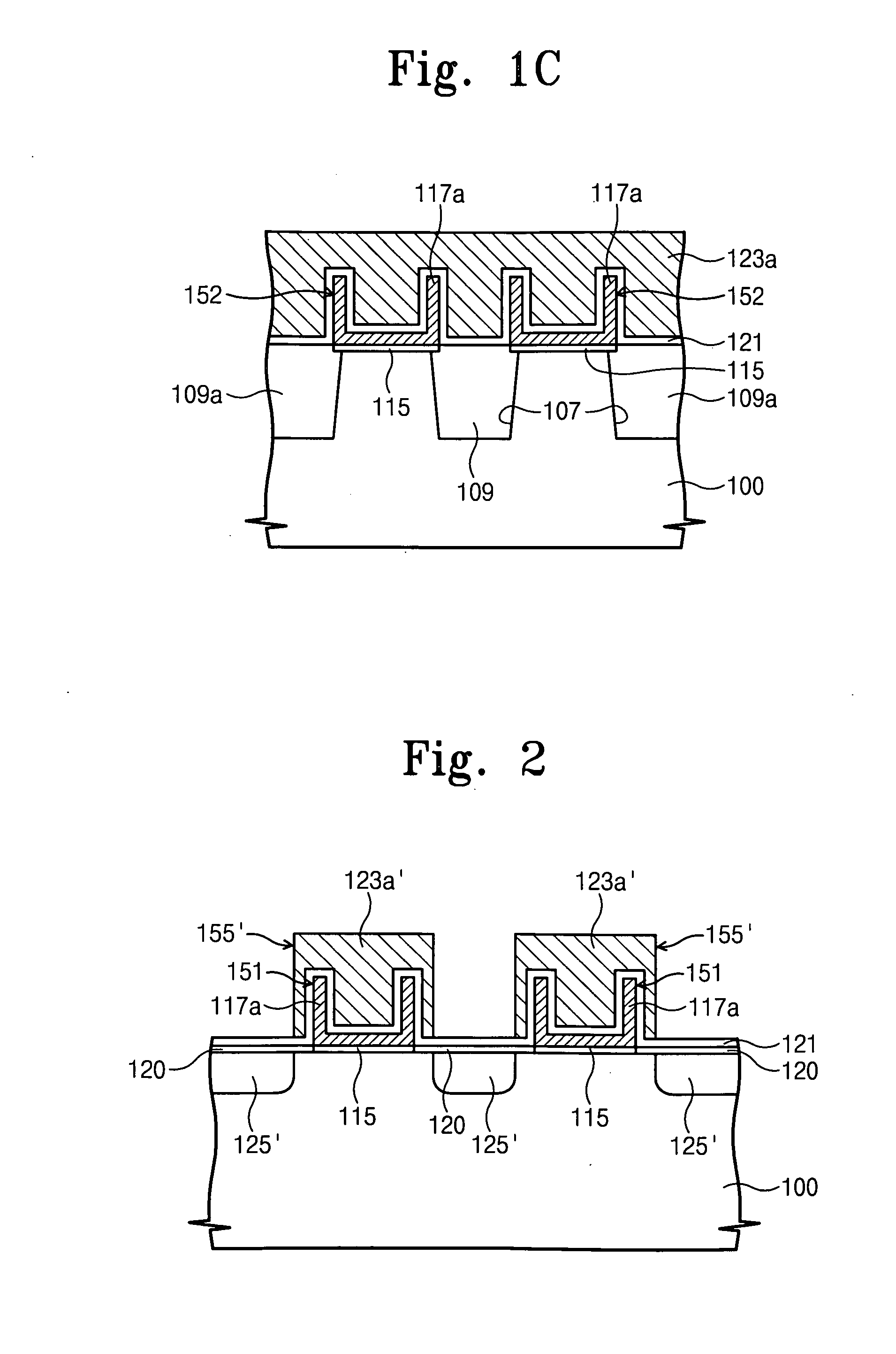
[0019]FIG. 1A is a top plan view of a non-volatile memory device according to an exemplary embodiment of the present invention. FIG. 1B and FIG. 1C are cross-sectional views taken along lines I-I′ and II-II′ of FIG. 1A, respectively.

[0020] Referring to FIG. 1A, FIG. 1B, and FIG. 1C, device isolation layers 109a are disposed on predetermined regions of a semiconductor substrate 1 to define active regions. The device isolation layers 109a may be linear when viewed from the top. Namely, the device isolation layers 109a are linearly. arranged on the semiconductor substrate 1 to run parallel with one another. Accordingly, the active regions may also be linear when viewed from the top. The device isolation l...


PUM


Abstract

A non-volatile memory device includes a device isolation layer disposed on a semiconductor substrate to define an active region, a floating gate disposed on the active region including a flat portion and a wall portion extending upwardly from an edge of the flat portion, a tunnel insulator interposed between the floating gate and the active region and a control gate electrode crossing over the active region and covering an inner side of the floating gate and at least a part of an outer side of the floating gate. The non-volatile memory device further includes a blocking insulator interposed between the control gate electrode and the floating gate.

Description

CROSS-REFERENCE TO RELATED APPLICATIONS [0001] This application claims priority from Korean Patent Application No. 10-2005-0048517, filed Jun. 7, 2005, the disclosure of which is hereby incorporated by reference herein in its entirety. BACKGROUND [0002] 1. Technical Field [0003] The present disclosure relates to a non-volatile memory device and methods of forming the same. More specifically, the present disclosure is directed to a non-volatile memory device having a floating gate and a method of forming the same. [0004] 2. Discussion of Related Art [0005] Non-volatile memory devices may retain their stored data even when their power supplies are interrupted. An example of a non-volatile memory device is the mask ROM non-volatile memory device. However, there are certain difficulties associated with mask ROM non-volatile memory devices in connection with their ability to erase and program data which has already been written. Accordingly, non-volatile memory devices which are sufficie...

Claims


Application Information

Patent Timeline
Patent Type & Authority Applications(United States)
IPC IPC(8): H01L29/788H01L21/336H10B69/00
CPCH01L21/28273H01L27/115H01L29/7881H01L29/42324H01L29/66825H01L27/11521H01L29/40114H10B69/00H10B41/30
Inventor JO, SANG-YOUN
Owner SAMSUNG ELECTRONICS CO LTD
Features
  • Generate Ideas
  • Intellectual Property
  • Life Sciences
  • Materials
  • Tech Scout
  • Unparalleled Data Quality
  • Higher Quality Content
  • 60% Fewer Hallucinations
Learn More