Multi-chip device and method for producing a multi-chip device

a multi-chip device and chip technology, applied in semiconductor devices, semiconductor/solid-state device details, electrical devices, etc., can solve the problems of limiting the number of stacked chips, affecting the overall height of the device, and increasing the total height of the chip stack

Inactive Publication Date: 2006-12-28
POLARIS INNOVATIONS LTD
View PDF2 Cites 116 Cited by
  • Summary
  • Abstract
  • Description
  • Claims
  • Application Information

AI Technical Summary

Problems solved by technology

The spacing between the chips may increase the total height of the chip stack and thereby may limit the number of stacked chips, for instance, due to size requirements of the package and bond wires or due to the stability of the multi-chip device.
The bond wire may require a spacing between the single chips of the chip stack, and the spacing for the bond wire may affect the overall height of the device.
The area provided for the substrate contact pads may be limited.
Thus, the overall number of contact pads on the first surface of the substrate may be limited, as well.

Method used


Image

  • Multi-chip device and method for producing a multi-chip device
  • Multi-chip device and method for producing a multi-chip device
  • Multi-chip device and method for producing a multi-chip device

Examples


Embodiment Construction

[0021] Embodiments of the invention generally provide multi-chip devices and methods of manufacturing the same.

[0022] While described below with respect to two or more memory devices in a multi-chip package, embodiments of the invention may be used to effect with any multi-chip package. The chips may be of the same type (e.g., both DRAMs) or different types. Likewise, the geometries may be different or the same in any given MCP. Although embodiments are described with respect to stacks having two dies (ICs) or four dies, any number of dies is contemplated. Furthermore, as used in this detailed description, directional terms such as, for example, upper, middle, lower, top, bottom, and over are used for convenience to describe a multi-chip package relative to one frame of reference regardless of how the multi-chip package may be oriented in space.

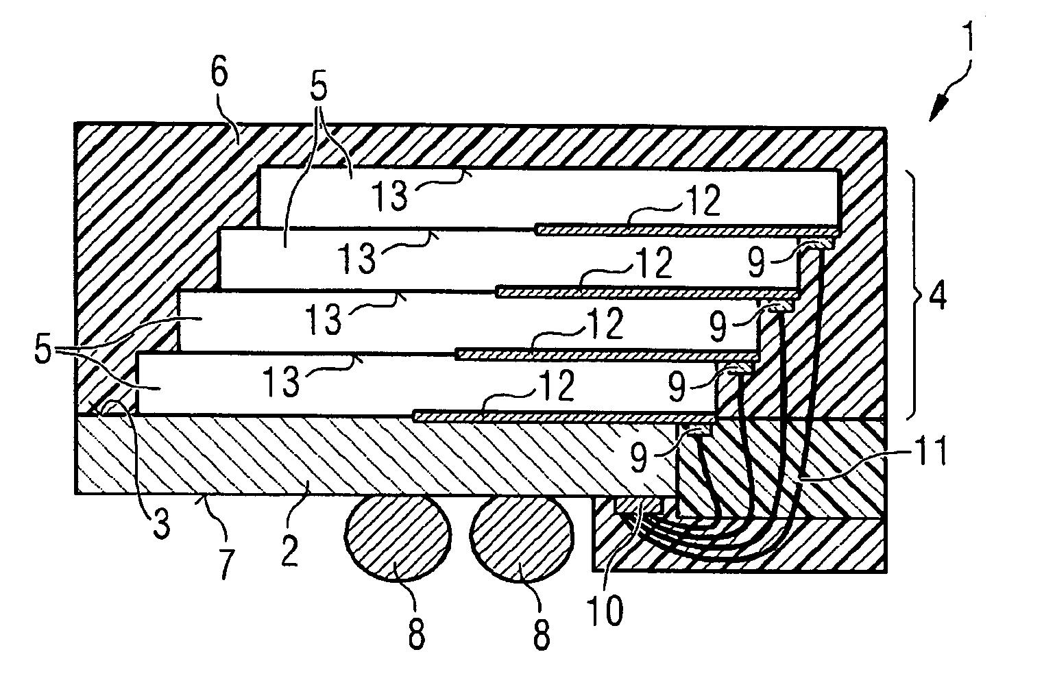
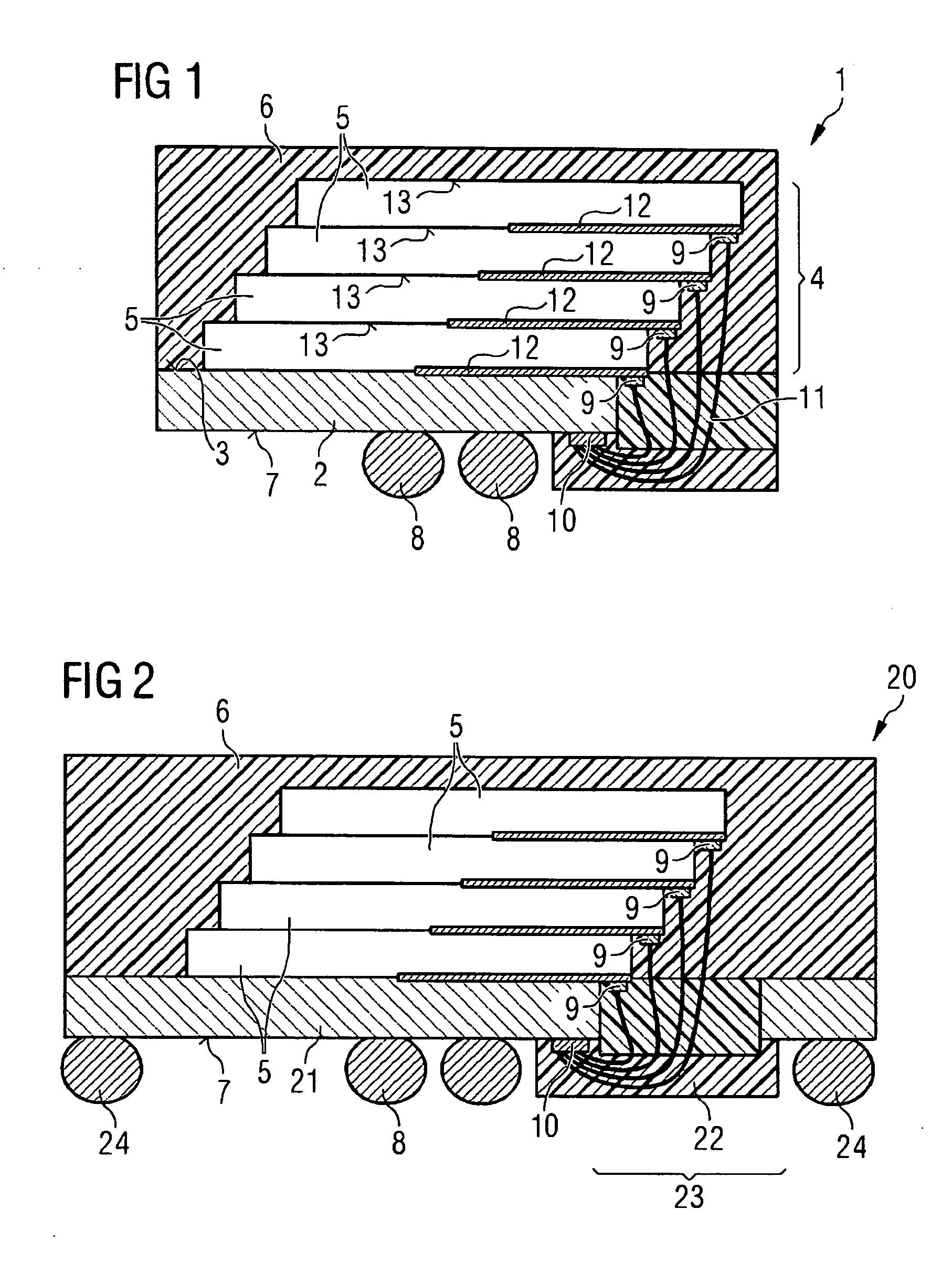
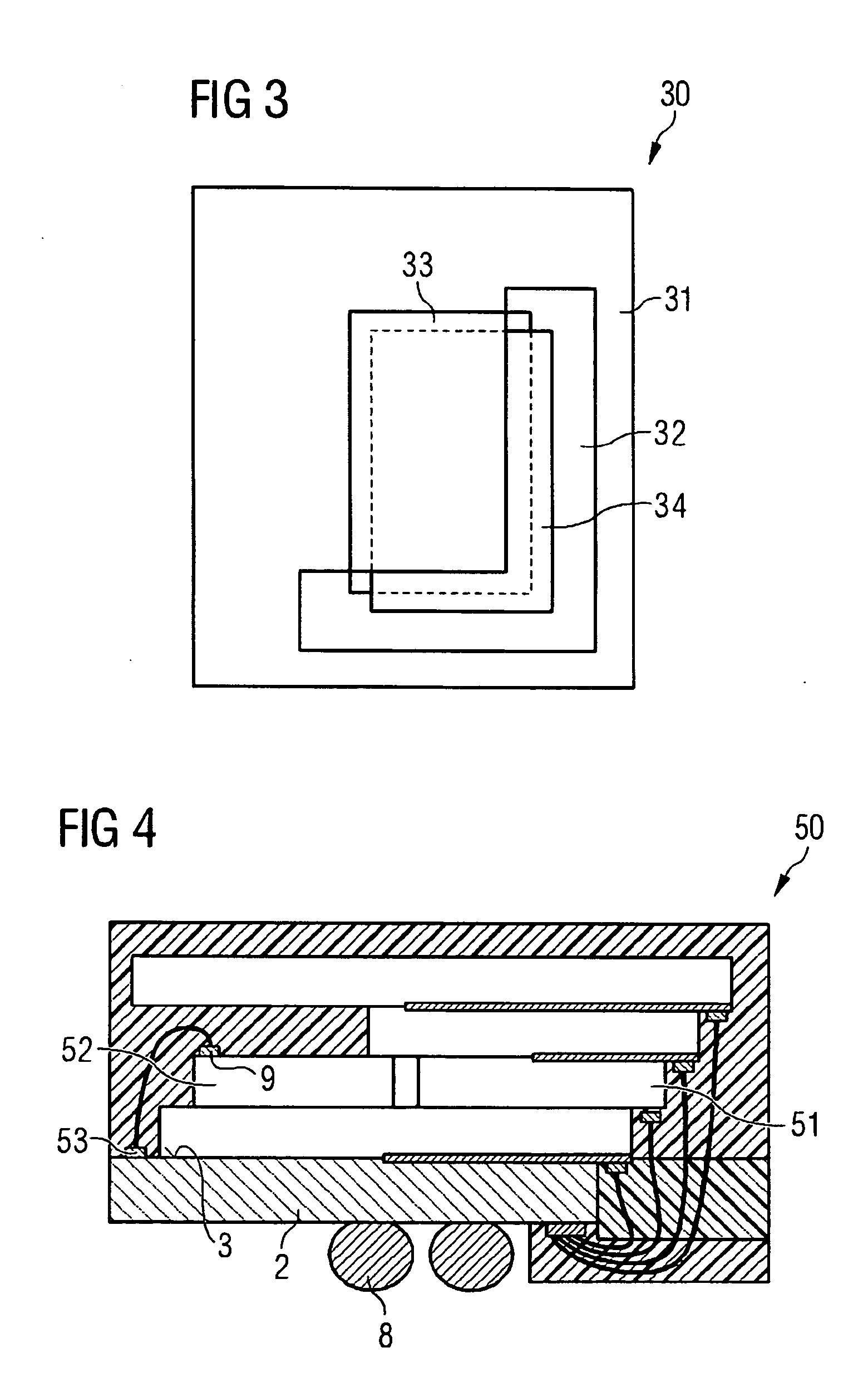
[0023] In FIG. 1, a cross-sectional view of a multi-chip device 1 according to one embodiment of the present invention is illustrated. The...


PUM


Abstract

The present invention relates to a multi-chip device comprising a substrate having a first surface on which a number of first contact elements is provided, a plurality of integrated circuit chips arranged in a chip stack which is arranged on a second surface of the substrate opposing the first surface, wherein each of the chips having a surface on which a number of second contact elements are provided, wherein a first one of the chips and the second contact elements thereon is arranged such that its second contact elements are uncovered by any of the chips or by the substrate and face towards the second surface of the substrate; and connecting elements which are arranged such as to connect at least one of the first contact elements of the substrate and at least one of the second contact elements of the first chip.

Description

BACKGROUND OF THE INVENTION [0001] 1. Field of the Invention [0002] The present invention relates to a multi-chip device and a method for producing a multi-chip device. [0003] 2. Description of the Related Art [0004] Memory storage capacity is usually provided by memory devices. To fulfill the market demands for higher storage density, memory devices have evolved into multi-chip devices (also referred to as multi-chip packages or MCPs) containing more than one memory chip in a single package. Because the increase of the memory density of memory chips may be limited, combining a plurality of memory chips in multi-chip memory devices may provide an efficient way to increase the density of memory devices according to the market demands. Also, for devices other than memory devices, an increased system density may be required such that a number of separately fabricated chips may be integrated into one device package. [0005] In some cases, the integration of chips in a multi-chip device u...

Claims


Application Information

Patent Timeline
Patent Type & Authority Applications(United States)
IPC IPC(8): H01L23/52
CPCH01L23/3128H01L2224/73215H01L2224/48091H01L2224/4824H01L2225/0651H01L2225/06541H01L2225/06562H01L2225/06586H01L2924/14H01L2924/15311H01L25/0657H01L2224/48227H01L2224/32225H01L24/48H01L2924/12041H01L2224/06135H01L2224/73265H01L2224/32145H01L2924/00014H01L2924/00012H01L2924/00H01L24/73H01L2224/023H01L2924/181H01L2224/45099H01L2224/45015H01L2924/207H01L2924/0001
Inventor THOMAS, JOCHENHETZEL, WOLFGANG
Owner POLARIS INNOVATIONS LTD
Why Eureka
Try Eureka