Method of correcting nonuniformity of pixels in an OLED

a display device and non-uniform technology, applied in the field of correction of non-uniform display in organic electroluminescence (el) display devices, can solve the problems of uneven light emission amount relative to input voltage (input voltage) among the pixels, and achieve accurate correction data, shorten the time considerably, and the effect of accurate correction data

Active Publication Date: 2007-01-11
GLOBAL OLED TECH
View PDF5 Cites 184 Cited by
  • Summary
  • Abstract
  • Description
  • Claims
  • Application Information

AI Technical Summary

Benefits of technology

[0017] According to the present invention, an area in which display unevenness exists is specified based on the photographed image, and the currents in the specified area and the currents of the peripheral pixels are measured to obtain accurate correction data. When there are many pixels, a relatively very long time is required to measure the currents of all of the pixels on a display panel, but, because the area to be measured can be specified by the present invention, it becomes possible to shorten the time considerably. Moreover, in an analysis using a photographed image, no quantitative measurements of luminance unevenness are necessary, and it is sufficient to know the rough position and the rough size of an area where unevenness exists, and no expensive and precise photography equipment is needed. Thus, when the size of an area in which luminance unevenness exists is comparatively small, or when luminance unevenness by a pixel or by a dot is corrected, correction data can be obtained effectively.

Problems solved by technology

Consequently, the threshold voltage Vth and the inclination of the V-I characteristic may vary among pixels due to manufacturing defects or tolerances, and the light emission amount relative to a data signal (input voltage) may become uneven among the pixels.

Method used


Image

  • Method of correcting nonuniformity of pixels in an OLED
  • Method of correcting nonuniformity of pixels in an OLED
  • Method of correcting nonuniformity of pixels in an OLED

Examples


Embodiment Construction

[0035] The preferred embodiment of the present invention is described below with reference to the attached drawings.

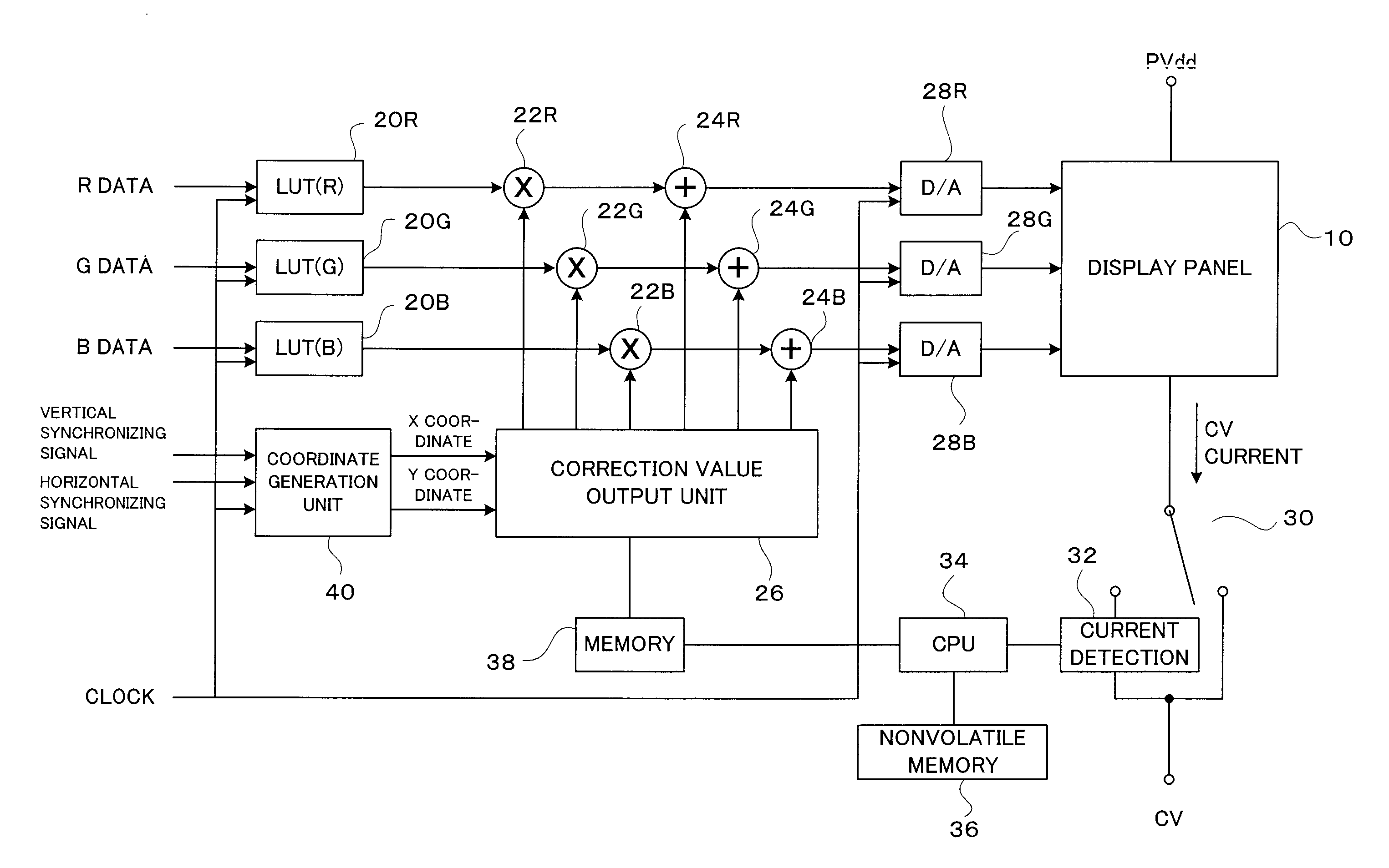
[0036]FIG. 4 shows the configuration of an organic EL display device correcting luminance data based on pre-stored correction data in order to supply the corrected luminance data to a display panel.

[0037] The display panel 10 includes pixels of each color of R, G and B, and input data (pixel data, or luminance data), which is a voltage signal relative to the luminance of each pixel, is independently input for each color of R, G and B. For example, when pixels of the same color are arranged in the vertical direction, data signals of any one of the R, G and B are supplied to each data line, and consequently display of all colors can be performed. It should be noted that, in this example, it is supposed that each set of data of R, G and B is luminance data of eight bits, and that the resolution of the display panel is 320 pixels in the horizontal direction and 240 lines...


PUM


Abstract

Nonuniformity in an organic EL display device is effectively detected. All display pixels of an organic EL panel are turned on and the display is photographed with a digital camera. A computer performs image processing of the photographed image to detect an area in which unevenness exists. Then, a V-I curve of each pixel in the area is measured to calculate necessary correction values. The calculated correction values are stored in a memory for use in correcting a signal input to the organic EL panel.

Description

FIELD OF THE INVENTION [0001] The present invention relates to correction of a nonuniformity of display in an organic electroluminescence (EL) display device formed by arranging organic EL elements in a matrix. BACKGROUND OF THE INVENTION [0002] Organic EL (OLED) display devices formed by arranging organic EL (OLED) elements in a matrix are conventionally well known. Among such displays, it is widely expected that a major stream of development of thin-shaped display devices will involve active type OLED display devices, in which the drive current for each OLED element is controlled by a transistor formed for each pixel. [0003]FIG. 1 shows an example of a pixel circuit of a conventional active type OLED display device. The source of a pixel driving P channel TFT 1 is connected to a power source PVdd, and the drain of the TFT 1 is connected to the anode of an organic EL (OLED) element 3, while the cathode of the OLED element 3 is connected to a negative power source CV. [0004] The gat...

Claims


Application Information

Patent Timeline
Patent Type & Authority Applications(United States)
IPC IPC(8): G09G3/30
CPCG09G3/3233G09G5/06G09G2300/0842G09G2320/0233G09G2360/147G09G2320/0285G09G2320/029G09G2320/043G09G2320/0242
Inventor KOHNO, MAKOTOONOMURA, KOUICHIMIZUKOSHI, SEIICHI
Owner GLOBAL OLED TECH
Why Eureka
Try Eureka