
Fixed abrasive pad having different real contact areas and fabrication method thereof

Inactive Publication Date: 2007-01-11
DONGBU ELECTRONICS CO LTD
View PDF3 Cites 0 Cited by
  • Summary
  • Abstract
  • Description
  • Claims
  • Application Information

AI Technical Summary

Benefits of technology

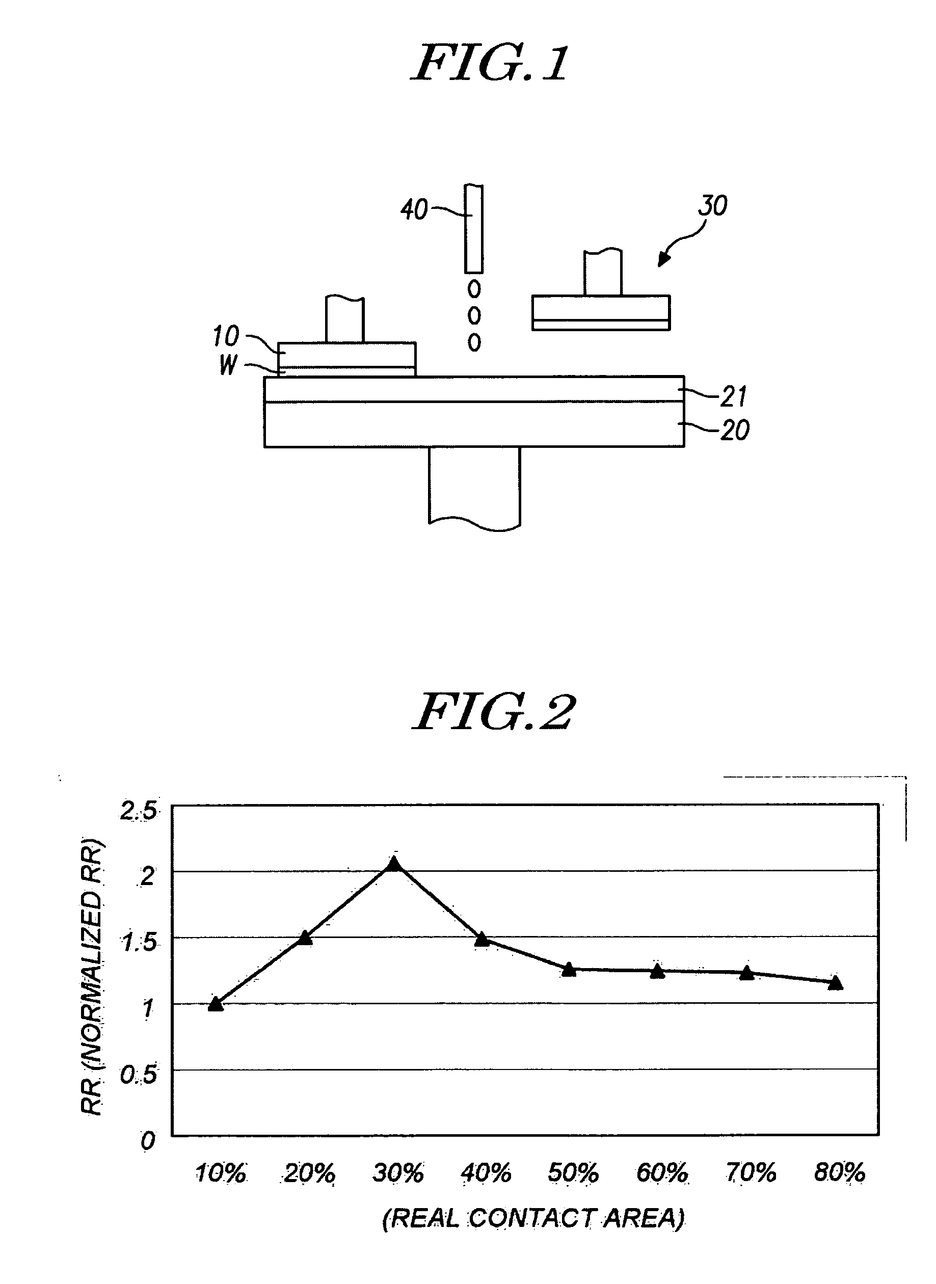
[0012] It is, therefore, an object of the present invention to provide a fixed abrasive pad comprising a plurality of polishing portions or areas in one pad. In use of a fixed abrasive pad according to the present invention, a wafer with a predetermined pattern is initially polished on a low real contact area (or low contact polishing portion) of the fixed abrasive pad. After polishing the patterned region of the wafer, the wafer is additionally polished on a high real contact area (or high contact polishing portion) of the fixed abrasive pad. Thereby, it can reduce or prevent adverse effects due to variations in removal rates according to the surface morphology of the wafer in a CMP process.

Problems solved by technology

The above-described CMP process has been widely used as a planarization process of metallization layers, however, the CMP process often results in a problem where the yield of semiconductor devices decreases due to failures such as a dishing or erosion phenomenon.
However, fabricating a roller by a cutting tool consumes a relatively large working time, and may also disable or disfigure the minute surface topology of the roller.
As a result, two different CMP apparatuses or equipment are necessary to simultaneously polish wafers with and without patterns, which is not desirable in the aspect of processing efficiency and / or efficient use of fab / clean room floor space.

Method used


Image

  • Fixed abrasive pad having different real contact areas and fabrication method thereof
  • Fixed abrasive pad having different real contact areas and fabrication method thereof
  • Fixed abrasive pad having different real contact areas and fabrication method thereof

Examples


first embodiment

A First Embodiment

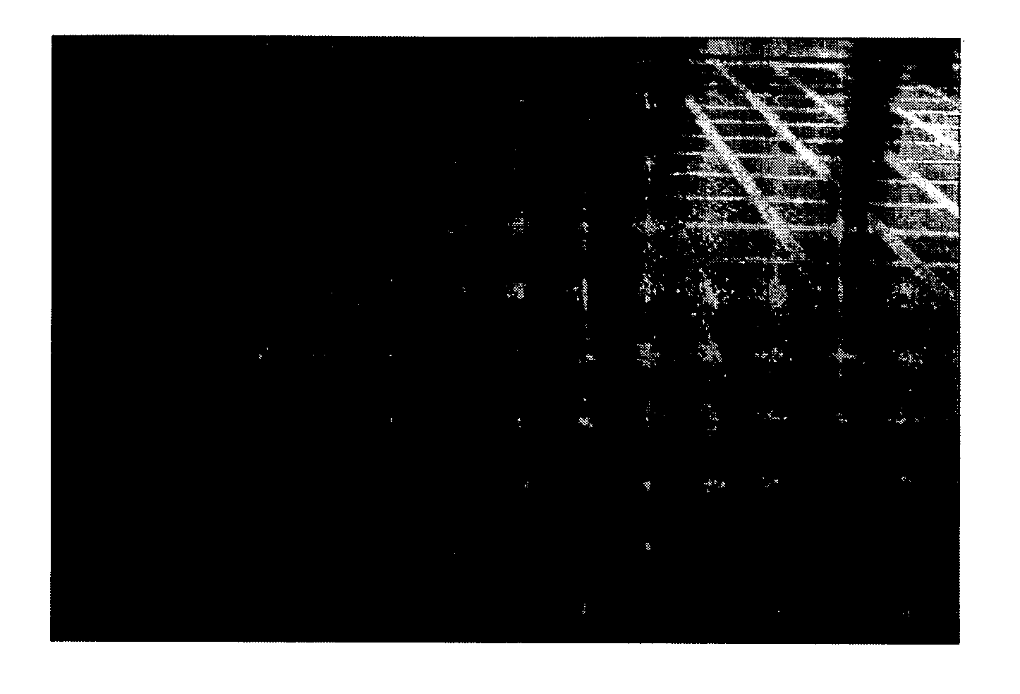
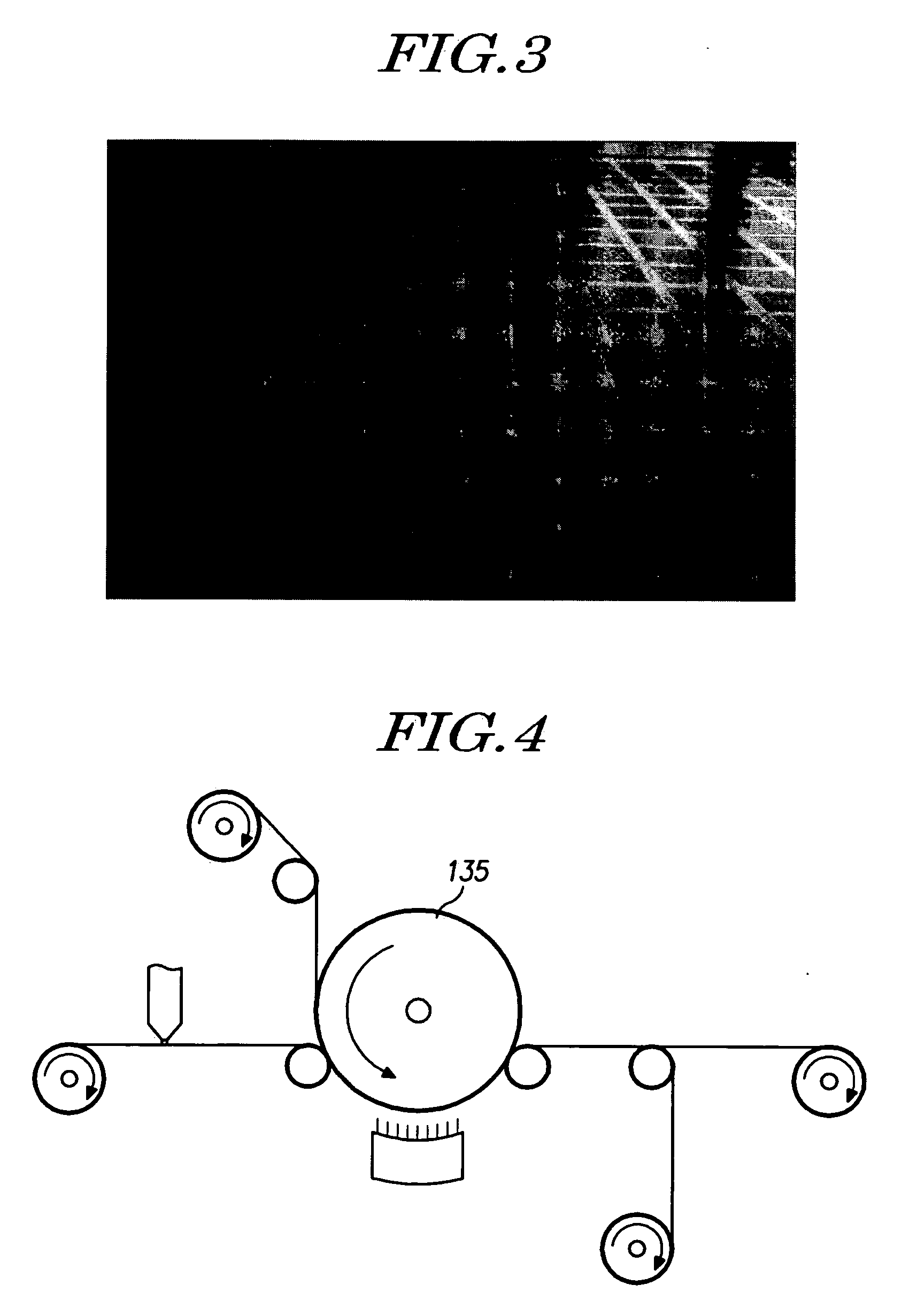
[0028] Firstly, an etching mold is formed, having a surface morphology opposite or complementary to the shape that is desired on a surface (e.g., the polishing surface) of the polishing pad. An exemplary etching mold is shown in FIG. 3. A metal material such as stainless steel is etched using a metal etching technique to form the mold, such as that shown in FIG. 3. The etching molds may be formed in at least two separate pieces, wherein one etching mold provides a polishing pad or pad region that has a different real contact area from another polishing pad or pad region. Alternatively, the mold may be formed in one unitary piece.

[0029] Next, the etching mold(s) providing different real contact areas are attached to a surface of roller. Preferably, the roller includes through-holes whereby a vacuum can be applied (e.g., to the inside of the roller), and the etching molds may be attached to the surface of the roller by a vacuum absorption mechanism.

[0030] A fixed a...

second embodiment

A Second Embodiment

[0035] The second embodiment of a method for fabricating a fixed abrasive pad having different real contact areas utilizes a press.

[0036] Firstly, a mixture of abrasive particles, a binding agent, and (optionally) a hardening agent is applied on a polycarbonate film constituting a base of the fixed abrasive pad, and then a polishing film is formed by a rolling method using a roller. Here, the roller has no surface morphology, and the polishing film is temporarily hardened in a constant thickness. Next, the etching molds having different real contact areas are respectively attached to a press.

[0037] Subsequently, the temporarily hardened polishing film is positioned on the press, and then is pressed or deformed by the press under a predetermined heat and pressure. After then, the polishing film is cooled, thus forming a fixed abrasive pad having one or more regions of relatively low real contact area and one or more regions of relatively high real contact area.

[...


PUM

PropertyMeasurementUnit
Fractionaaaaaaaaaa
Fractionaaaaaaaaaa
Densityaaaaaaaaaa

Abstract

Disclosed is a method for fabricating a fixed abrasive pad in use of a chemical mechanical polishing process. The method includes: forming one or more etching molds providing a plurality of different real contact areas; attaching the etching mold(s) to a roller or press; and forming a fixed abrasive pad using the roller or press, The fixed abrasive pad has a plurality of polishing portions, each having a different real contact area. Especially, the fixed abrasive pad can comprise a low-density polishing portion having a real contact area less than 20% and a high-density polishing portion having a real contact area of 20%-50%.

Description

[0001] This application claims the benefit of Korean Application No. 10-2005-0061837, filed on Jul. 8, 2005, which is incorporated by reference herein in its entirety. BACKGROUND OF THE INVENTION [0002] 1. Field of the Invention [0003] The present invention relates to a fixed abrasive pad and fabrication method thereof. More specifically, the present method relates to a fixed abrasive pad having different real contact areas in use in a chemical mechanical polishing (CMP) process, and a method for forming different real contact areas on a fixed abrasive pad. [0004] 2. Description of the Related Art [0005] There have been a variety of alterations in structural and material aspects for the purpose of achieving a higher operational speed and integration of a semiconductor device. In the structural aspect, the number of metallization layers has been increased, and a shallow trench isolation (STI) technique has been employed. In the material aspect, copper (Cu) has been used as a metalliz...

Claims


Application Information

Patent Timeline
IPC IPC(8): B24B7/30B24B1/00B24B29/00B24D11/00
CPCB24D11/001H01L21/304
Inventor CHOI, JAE YOUNG
Owner DONGBU ELECTRONICS CO LTD
Learn More