Array substrate for in-plane switching liquid crystal display device with polycrystalline silicon pixel electrode and method of manufacturing the same

a liquid crystal display and polycrystalline silicon technology, applied in non-linear optics, instruments, optics, etc., can solve the problems of narrow viewing angle, critical dimension (cd), and conventional lcd devices with longitudinal electric fields, so as to increase the aperture ratio and reduce the manufacturing process

Active Publication Date: 2007-01-18
LG DISPLAY CO LTD
View PDF1 Cites 37 Cited by
  • Summary
  • Abstract
  • Description
  • Claims
  • Application Information

AI Technical Summary

Benefits of technology

[0026] An advantage of the present invention is to provide an array substrate for an in-plane switching liquid crystal display device and a method of fabricating the same, which increase an aperture ratio.
[0027] Another advantage of the present invention is to provide an array substrate for an in-plane switching liquid crystal display device and a method of fabricating the same, which has a uniform critical dimension.
[0028] Another advantage of the present invention is to provide an array substrate for an in-plane switching liquid crystal display device and a method of fabricating the same, which reduces manufacturing processes.

Problems solved by technology

However, the conventional LCD devices having the longitudinal electric field have a drawback in that they have a very narrow viewing angle.
Selection of the transparent conducting material as an electrode material for improving the aperture ratio may have the following problems.
A critical dimension (CD), which may be defined as a design rule of a pattern in the panel, may be non-uniform in each region due to the wet etching process.
In addition, since the transparent conducting material transmits light, scratches on a back surface of the substrate by a chuck for supporting the substrate may have large effects on an exposing process of the substrate, whereby patterns having uneven sides may be formed.
If the common and pixel electrodes are formed of the transparent conducting material, more processes for forming contact holes may be needed, and thus problems may be increased.

Method used


Image

  • Array substrate for in-plane switching liquid crystal display device with polycrystalline silicon pixel electrode and method of manufacturing the same
  • Array substrate for in-plane switching liquid crystal display device with polycrystalline silicon pixel electrode and method of manufacturing the same
  • Array substrate for in-plane switching liquid crystal display device with polycrystalline silicon pixel electrode and method of manufacturing the same

Examples


first embodiment

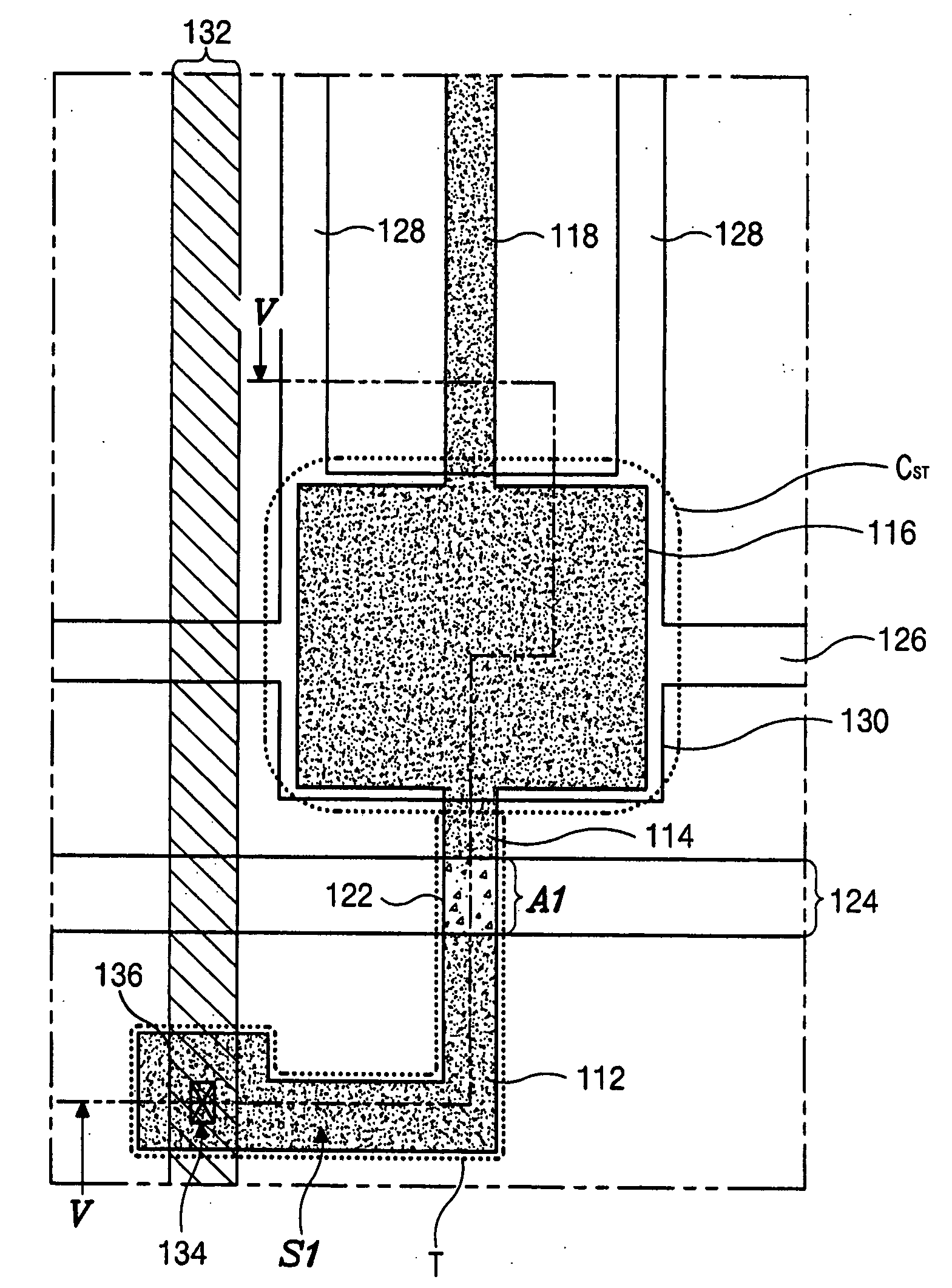
[0049]FIG. 4 is a plan view illustrating an array substrate for an IPS-LCD device according to the present invention. The array substrate includes a top gate type thin film transistor.

[0050] As shown in FIG. 4, a gate line 124 is formed in a first direction and a data line 132 is formed in a second direction crossing the first direction. The gate line 124 and the data line 132 cross each other to define a pixel region P.

[0051] A semiconductor layer 112 is formed to overlap the gate line 124 and the data line 132. A first capacitor electrode 116 and a pixel electrode 118 are formed in the pixel region P. The pixel electrode 118 connected to the first capacitor electrode 116 is formed parallel to the data line 132. A drain electrode 114 is interposed between the semiconductor layer 112 and the first capacitor electrode 116. The semiconductor layer 112 includes an active area A1 and a source area S1. The active area A1 overlaps the gate line 124, and an overlapped portion of the gate ...

second embodiment

[0075]FIG. 8 is a plan view illustrating an array substrate for an IPS-LCD device according to the present invention.

[0076] In FIG. 8, a gate line 224 including a gate electrode 222 and a data line 232 including a source electrode 236 are formed to cross each other. The gate and data lines 224 and 236, respectively, define a pixel region P. A semiconductor layer 212 is formed to overlap the gate electrode 222 and the source electrode 236. A first capacitor electrode 216 is formed in the pixel region P and a pixel electrode 218 is formed substantially parallel to the data line 232. A drain electrode 214 is formed between the semiconductor layer 212 and the first capacitor electrode 216. The semiconductor layer 212, the drain electrode 214, the first capacitor electrode 216 and the pixel electrode 218 are made of polycrystalline silicon and are formed as a unit during the same process. The source electrode 236 is connected to the semiconductor layer 212 through a source contact hole 2...

third embodiment

[0089]FIG. 10 is a plan view illustrating an array substrate for an IPS-LCD according to the present invention.

[0090] In FIG. 10, a gate line 314 including a gate electrode 312 is formed in a first direction, and a data line 332 including a source electrode 330 is formed in a second direction. The gate line 314 and the data line 332 cross each other to define a pixel region P. The gate electrode 312 extends from the gate line 314 in the second direction and the source electrode 330 extends from the data line 332 in the first direction. The source electrode 330 overlaps the gate electrode 312 by a distance. A common line 318 is formed substantially in parallel to the gate line 314. A first capacitor electrode 316 and a plurality of common electrodes 320 are formed in the pixel region P and are connected to the common line 318. The plurality of common electrodes 320 is substantially parallel to the data line 332. The common line 318, the first capacitor electrode 316 and the common el...


PUM

PropertyMeasurementUnit
angleaaaaaaaaaa
source areaaaaaaaaaaa
areaaaaaaaaaaa

Abstract

An array substrate for in-plane switching liquid crystal display device includes a gate line on a substrate, a data line crossing the gate line to define a pixel region, a semiconductor layer including an active area and a source area, wherein the active area overlaps the gate line and the source area overlaps the data line, a drain electrode connected to the semiconductor layer, a first capacitor electrode in the pixel region and connected to the drain electrode, a pixel electrode connected to the first capacitor electrode and substantially in parallel to the data line, a common line substantially parallel to the gate line, a second capacitor electrode connected to the common line and overlapping the first capacitor electrode, and a common electrode connected to the common line and alternatively arranged with the pixel electrode, wherein the source area of the semiconductive layer, the drain electrode, the first capacitor electrode and the pixel electrode include doped polycrystalline silicon.

Description

[0001] This application claims the benefit of Korean Patent Application No. 2003-0017476, filed on Mar. 20, 2003, which is hereby incorporated by reference as if fully set forth herein. BACKGROUND OF THE INVENTION [0002] 1. Field of the Invention [0003] The present invention relates to a liquid crystal display device, and more particularly, to an array substrate for an in-plane switching (IPS) liquid crystal display device and a method of fabricating the same. [0004] 2. Discussion of the Related Art [0005] A liquid crystal display device uses the optical anisotropy and polarization properties of liquid crystal molecules to produce an image. Liquid crystal molecules have a definite orientational alignment as a result of their long, thin shapes. That alignment direction can be controlled by an applied electric field. In other words, as an applied electric field changes, so does the alignment of the liquid crystal molecules. Due to the optical anisotropy, the refraction of incident lig...

Claims


Application Information

Patent Timeline
Patent Type & Authority Applications(United States)
IPC IPC(8): G02F1/1343G02F1/1362
CPCG02F1/134363G02F2201/40G02F1/136213G02F1/1343
Inventor JEOUNG, HUN
Owner LG DISPLAY CO LTD
Why Eureka
Try Eureka