Supercharge Your Innovation With Domain-Expert AI Agents!

Packaging for high speed integrated circuits

a technology of integrated circuits and packaging, applied in the direction of semiconductor devices, semiconductor/solid-state device details, electrical apparatus, etc., can solve the problems of data errors, reduced design margins to an unacceptable level, and pair coupling problems that are even greater for low-speed devices

Active Publication Date: 2007-01-25
MARVELL ASIA PTE LTD
View PDF32 Cites 7 Cited by
  • Summary
  • Abstract
  • Description
  • Claims
  • Application Information

AI Technical Summary

Benefits of technology

[0075] In other features, the method comprises spacing the first and second leads and the third and fourth leads at a first distance; and spacing the second and third leads at a second distance that is different than the first distance. The method comprises carrying high speed differential signals using the first and second leads and the third and fourth leads of the lead frame. The high speed differential signals have a frequency greater than or equal to 1 Gigabit per second (Gb/s). The lead frame further comprises a fifth lead and furt

Problems solved by technology

The magnitude of the difference between the signals carried on the adjacent pairs tends to cause data errors and / or to reduce design margins to an unacceptable level particularly for high speed signals such as Gigabit per second and higher data rates.
The pair coupling problem tends to be even greater for low cost plastic lead frames as compared to ball grid array (BGA) packaging with a ground plane shield.

Method used


Image

  • Packaging for high speed integrated circuits
  • Packaging for high speed integrated circuits
  • Packaging for high speed integrated circuits

Examples


Embodiment Construction

[0111] The following description of the preferred embodiment(s) is merely exemplary in nature and is in no way intended to limit the invention, its application, or uses. For purposes of clarity, the same reference numbers will be used in the drawings to identify similar elements.

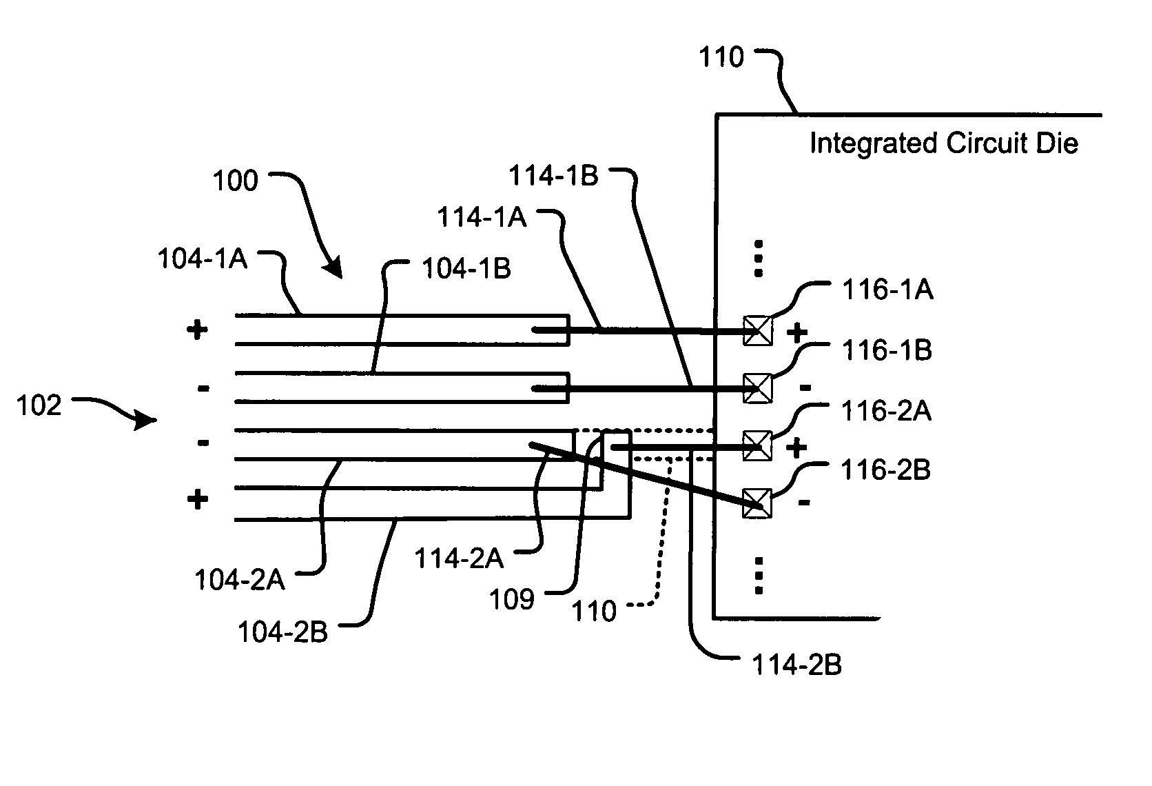
[0112] The present invention reduces pair coupling of differential lines operating at high speeds. Referring now to FIG. 4, differential signal pairs are connected by leads of a lead frame and bondwires to pads of the IC according to one implementation of the present invention. A lead frame 100 comprises one or more sets 102 of leads 104 including a first pair of leads 104-1 A and 104-2B and a second pair of leads 104-2A and 104-2B (collectively leads 104). The lead 104-1A is located adjacent to the lead 104-1B, the lead 104-1B is located adjacent to the lead 104-2A, and the lead 104-2A is located adjacent to the lead 104-2B.

[0113] The lead 104-1A carries a signal having a first polarity, the lead 104-1B c...


PUM


Abstract

An integrated circuit package comprises an integrated circuit die comprising N adjacent pads, where N is an integer greater than three. A substrate comprises a first pair of traces including first and second traces and a second pair of traces including third and fourth traces. The first, second, third and fourth traces include first ends spaced from the integrated circuit die and second ends adjacent to the integrated circuit die. The first and second pairs of traces carry differential signals. The third trace of the second pair of traces has a first polarity and the fourth trace of the second pair of traces has a second polarity. The third trace is located on one side of the fourth trace at the first end and is located on an opposite side of the fourth trace at the second end. N connections independently connect the second ends to N pads.

Description

CROSS-REFERENCE TO RELATED APPLICATIONS [0001] This application is a continuation of U.S. patent application Ser. No. 11 / 248,985 filed on Oct. 12, 2005, and claims the benefit of U.S. Provisional Application Nos. 60 / 722,272, filed on Sep. 30, 2005 and 60 / 701,701, filed on Jul. 22, 2005. The disclosures of the above applications are incorporated herein by reference in its entirety.FIELD OF THE INVENTION [0002] The present invention relates to packaging for integrated circuits (ICs), and more particularly high speed packaging for ICs. BACKGROUND OF THE INVENTION [0003] Modern integrated circuits (ICs) typically employ differential signaling. In differential signaling, a signal is conveyed between two separate, active conductors instead of one active conductor and ground. The magnitude of the differential signal is the difference between the two signals rather than the voltages between the two individual signals and ground. [0004] To transmit or receive differential signals to or from ...

Claims


Application Information

Patent Timeline
IPC IPC(8): H01L23/48
CPCH01L23/495H01L2924/07802H01L23/49558H01L23/49816H01L23/49838H01L23/50H01L23/552H01L23/66H01L24/49H01L2223/6611H01L2223/6638H01L2224/16H01L2224/48091H01L2224/4813H01L2224/48227H01L2224/48247H01L2224/4826H01L2224/48465H01L2224/48472H01L2224/49113H01L2224/4917H01L2224/49171H01L2224/49175H01L2224/49177H01L2224/4943H01L2924/01005H01L2924/01013H01L2924/01027H01L2924/01029H01L2924/0105H01L2924/01082H01L2924/14H01L2924/15311H01L2924/19051H01L2924/19107H01L2924/30105H01L2924/30107H01L2924/3011H01L2924/3025H01L23/49541H01L2224/16225H01L2924/014H01L2924/01033H01L2924/01006H01L24/48H01L2924/00014H01L2924/00H01L2924/30111H01L2924/181H01L2224/05554H01L2224/45099H01L2224/05599H01L2924/00012
Inventor SUTARDJA, SEHAT
Owner MARVELL ASIA PTE LTD
Features
  • R&D
  • Intellectual Property
  • Life Sciences
  • Materials
  • Tech Scout
  • Unparalleled Data Quality
  • Higher Quality Content
  • 60% Fewer Hallucinations
Learn More