
Semiconductor device

a technology of semiconductor devices and semiconductors, applied in semiconductor devices, semiconductor/solid-state device details, electrical apparatus, etc., can solve the problem of not getting the correct result at detecting whether the electric fuse is cut, and achieve the effect of easy heating and easy heating

Active Publication Date: 2007-03-08
RENESAS ELECTRONICS CORP
View PDF3 Cites 26 Cited by
  • Summary
  • Abstract
  • Description
  • Claims
  • Application Information

AI Technical Summary

Benefits of technology

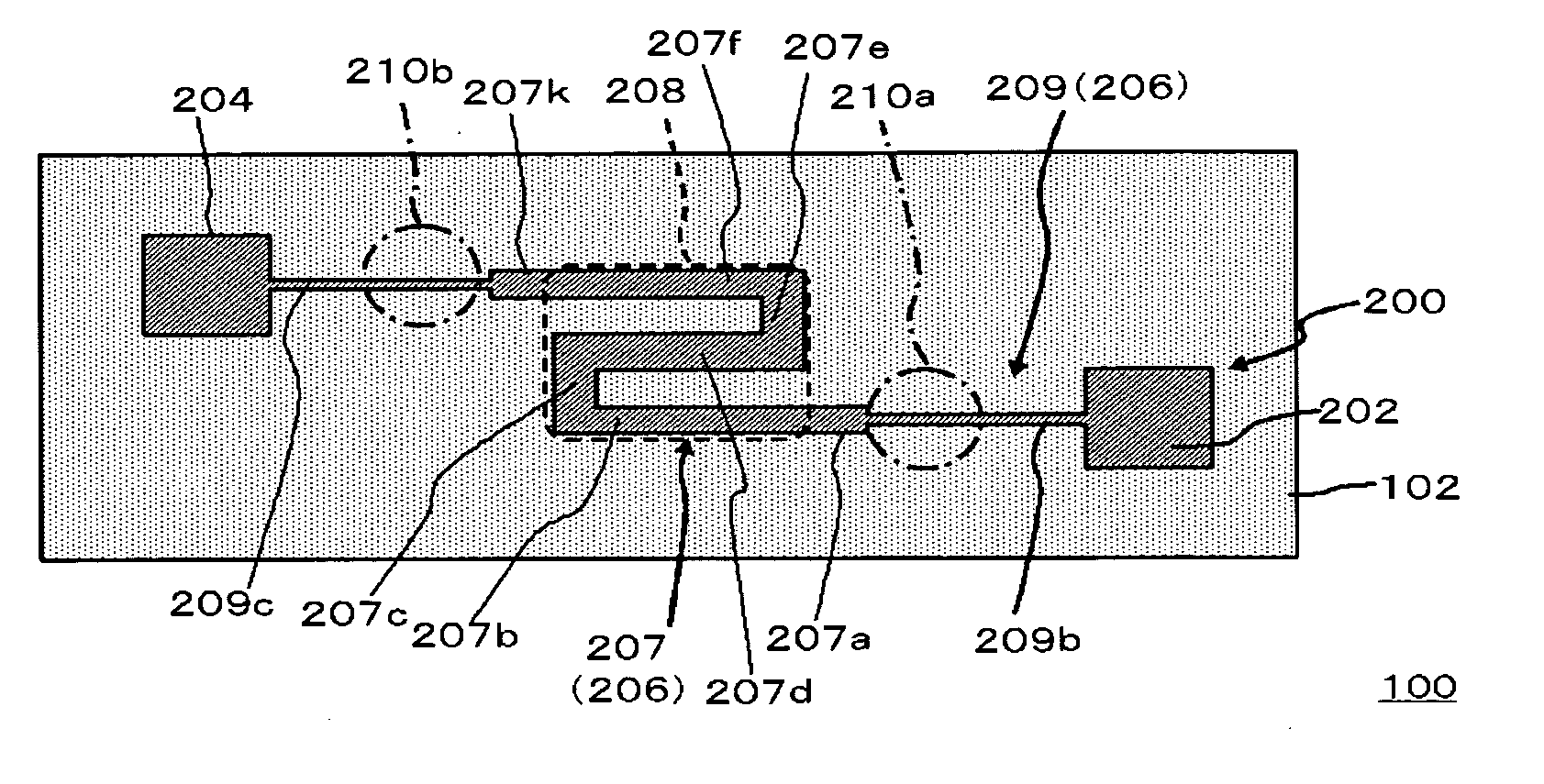
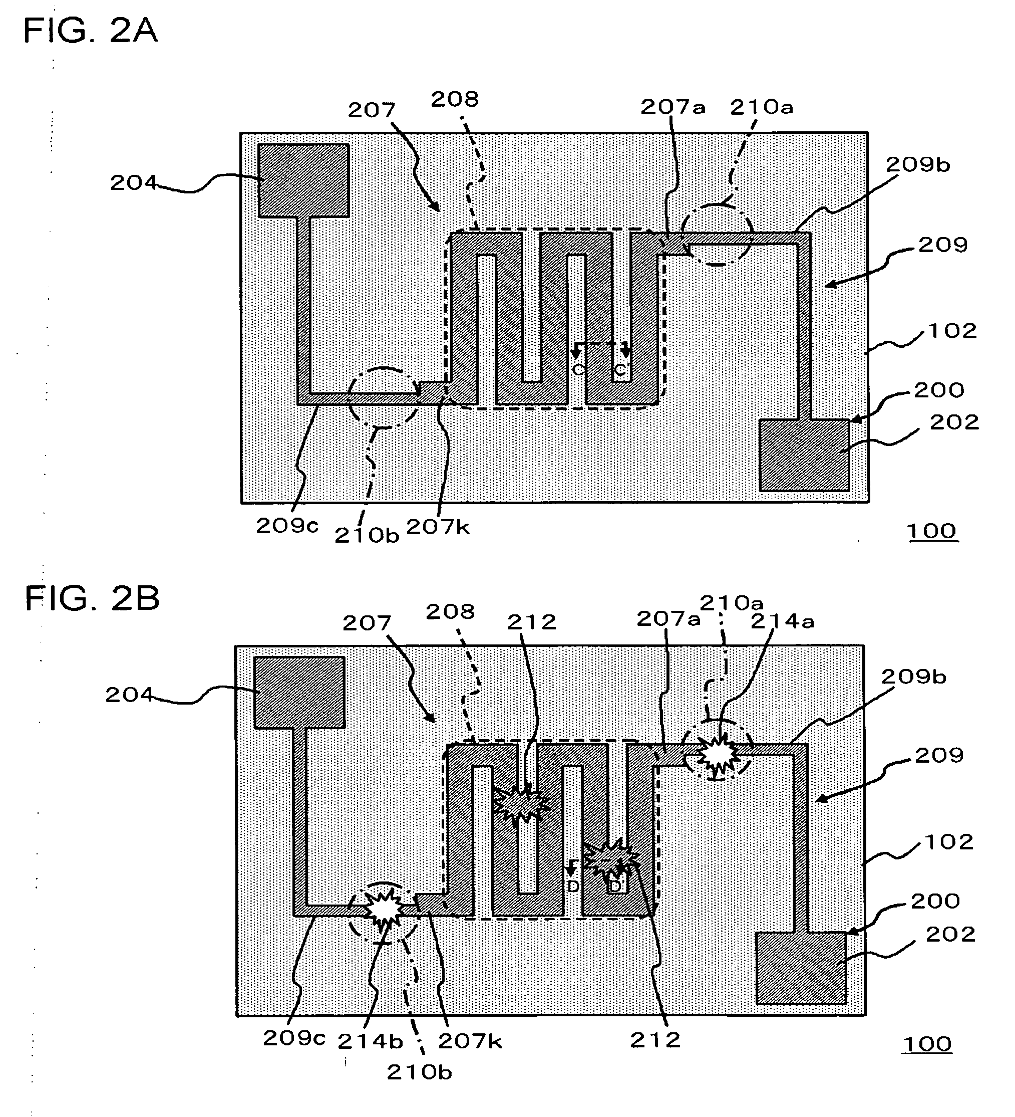
[0015] According to the semiconductor device of the present invention, material forming the fuse is easily heated in the region, in which a plurality of straight line portions are juxtaposed with each other by folding the first interconnect, when a current is applied to the electric fuse. On the other hand, as the second interconnect having a narrower width than that of the first interconnect is connected to the first interconnect outside the region, cutting may be executed on that location. According to the above-described configuration, cutting may be promoted by providing a location in which the electric fuse is easily heated, a location in which cutting is performed may be formed at a location different from a location which is easily heated, therefore a state in which the electric fuse is cut, may be preferably held.

Problems solved by technology

If such reconnection is caused, a correct result will not be obtained at detecting whether the electric fuse is cut even if the electric fuse to be cut has been cut.

Method used


Image

  • Semiconductor device
  • Semiconductor device
  • Semiconductor device

Examples


first embodiment

(First Embodiment)

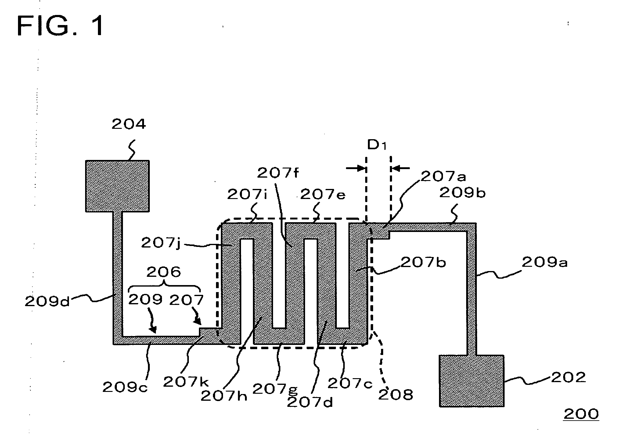
[0071]FIG. 1 is a plan view showing the configuration of an electric fuse included in a semiconductor device according to the present embodiment.

[0072] An electric fuse 200 includes: a conductive member 206 formed with a wide interconnect 207 (first interconnect), and a narrow interconnect 209 (second interconnect); a first terminal 202 formed at one end; and a second terminal 204 formed at the other end of the conductive member 206. The narrow interconnect 209 is formed as a narrower interconnect width than that of the wide interconnect 207, wherein the interconnect width represents an interconnect width approximately perpendicular to a current direction (hereinafter, simply called “interconnect width”). Moreover, the electric fuse 200 has a juxtaposed region 208 in which a plurality of straight line portions are juxtaposed with each other by folding of the wide interconnect 207. In the present embodiment, the electric fuse 200 is an electric fuse (E fuse) in whi...

second embodiment

(Second Embodiment)

[0107]FIG. 14A and 14B are plan views showing one example of the configuration of the semiconductor device 100 according to the present embodiment. FIG. 14A shows one example of the configuration of the electric fuse 200 before cutting, and FIG. 14B shows one example of the configuration of the electric fuse 200 after cutting.

[0108] The configuration of the present embodiment is different from that of the electric fuse 200 shown in the first embodiment in a point that the narrow interconnect 209 is provided only on the side of the second terminal 204, and the wide interconnect 207 is directly connected to the first terminal 202. Here, the wide connecting portion 207l, the folded structure of the wide interconnect 207, the separation portion 207k, and the narrow interconnect 209 are connected in this order between the first terminal 202 and the second terminal 204.

[0109] In the above-described configuration, the expected cut region 210 is provided on the narrow i...

third embodiment

(Third Embodiment)

[0118]FIG. 16 is a plan view showing one example of the configuration of the semiconductor device 100 according to the present embodiment. Here, the drawing shows one example of the configuration of the electric fuse 200 before cutting.

[0119] The electric fuse 200 of the present embodiment is different from that in the semiconductor device 100 shown in the first and second embodiments in a point that the wide interconnect 207A with the folded structure is connected to the first terminal 202, the wide interconnect 207B with the folded structure is connected to the second terminal 204, and the narrow interconnect 209 is provided between the wide interconnect 207A and the wide interconnect 207B. The wide interconnect 207A has a structure in which the separation portion 207m is provided at the connecting portion to the narrow interconnect 209, and the wide interconnect 207B has a structure in which the separation portion 207n is provided at the connecting portion to t...


PUM


Abstract

An electric fuse includes a wide interconnect and a narrow interconnect. The electric fuse has a juxtaposed region in which a plurality of straight line portions are juxtaposed with each other by folding the wide interconnect and the narrow interconnect has a narrower width than that of the wide interconnect, and, at the same time, is connected to the wide interconnect outside the juxtaposed region.

Description

[0001] This application is based on Japanese Patent application NO. 2005-256787, the content of which is incorporated hereinto by reference. BACKGROUND OF THE INVENTION [0002] 1. Technical Field [0003] The present invention relates to a semiconductor device, and, more particularly, to a semiconductor device including an electric fuse. [0004] 2. Related Art [0005] Conventionally, there has been known a technology according to which a fuse is installed in a semiconductor device, the fuse is cut to adjust a resistance value used in the semiconductor device, to remove a defective element for replacement by a normal element, and the like. [0006] In order to cut or disconnect a fuse, there has been used a method, by which a fuse is cut by irradiating a part of the fuse with beams of laser light, or a method of cutting a fuse by use of an electric current. [0007] Japanese Laid-open patent publication No. 2005-39220 has disclosed a fuse which can be cut by a smaller current. In Japanese Lai...

Claims


Application Information

Patent Timeline
IPC IPC(8): H01L29/00
CPCH01L23/5256H01L2924/0002H01L2924/00
Inventor UEDA, TAKEHIRO
Owner RENESAS ELECTRONICS CORP
Learn More