
Transistor design self-aligned to contact

Active Publication Date: 2007-03-15
TEXAS INSTR INC
View PDF12 Cites 7 Cited by
  • Summary
  • Abstract
  • Description
  • Claims
  • Application Information

AI Technical Summary

Problems solved by technology

First, the cost per functional unit should drop with each generation of complexity so that the cost of the product with its doubled functionality would increase only slightly.
Second, the higher product complexity should largely be achieved by shrinking the feature sizes of the chip components while holding the package dimensions constant; preferably, even the packages should shrink.
Third, the increased functional complexity should be paralleled by an equivalent increase in reliability of the product.
One area of integrated circuit manufacturing technology that poses difficulties in continued miniaturization and cost reduction is that of making electrical contact to a transistor device.
When the contact does hit the spacer, the area of electrically conductive contact to the substrate is reduced, leading to increased resistance of the contact and resulting yield fallout.
A second concern to the manufacturer is the cost associated with pattering levels in the manufacturing process.
When the cost of prototype designs is included in the total cost of a semiconductor product, the cost of multiple revisions, each requiring several minimum geometry masks, can be significant.

Method used


Image

  • Transistor design self-aligned to contact
  • Transistor design self-aligned to contact
  • Transistor design self-aligned to contact

Examples


Embodiment Construction

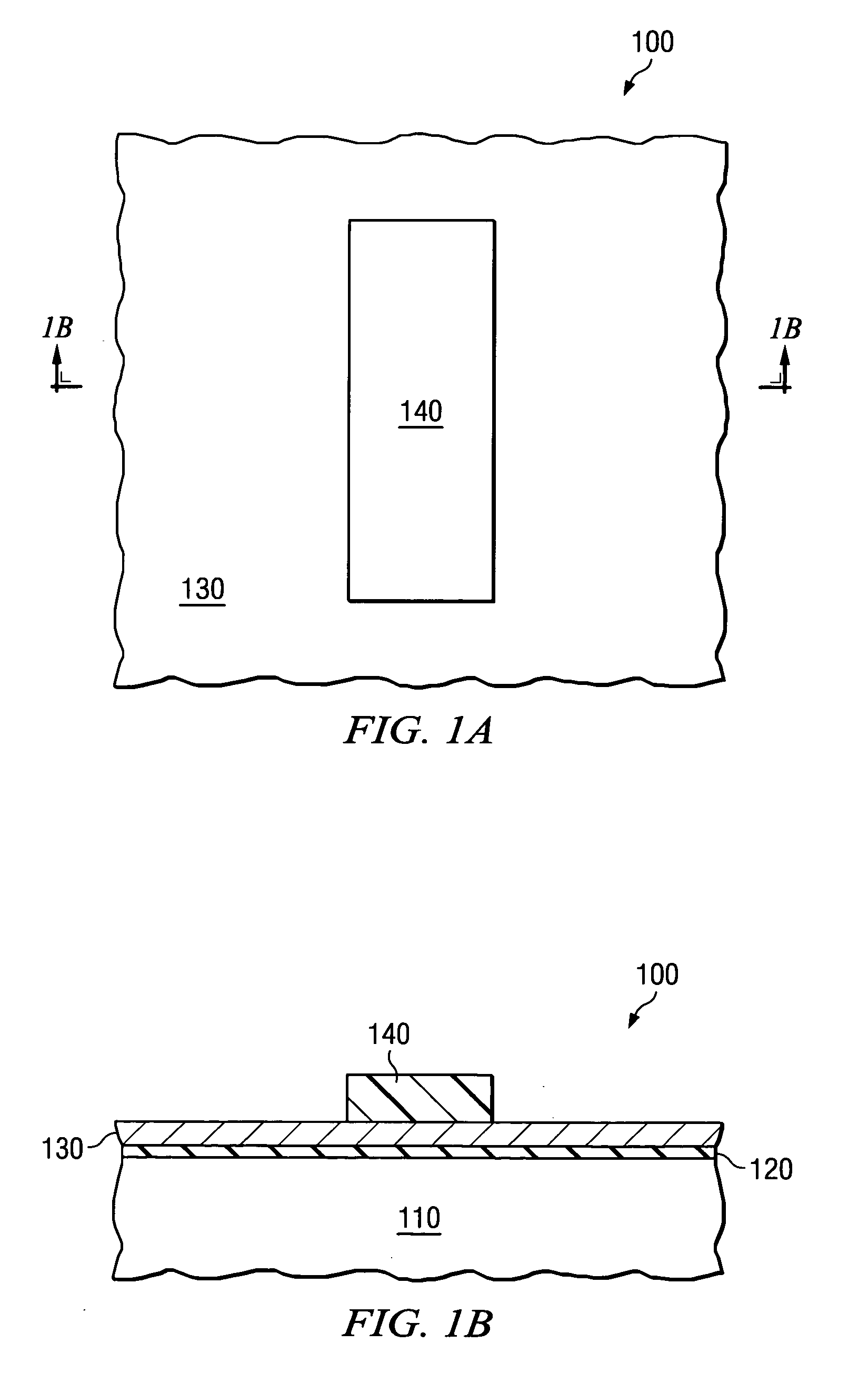
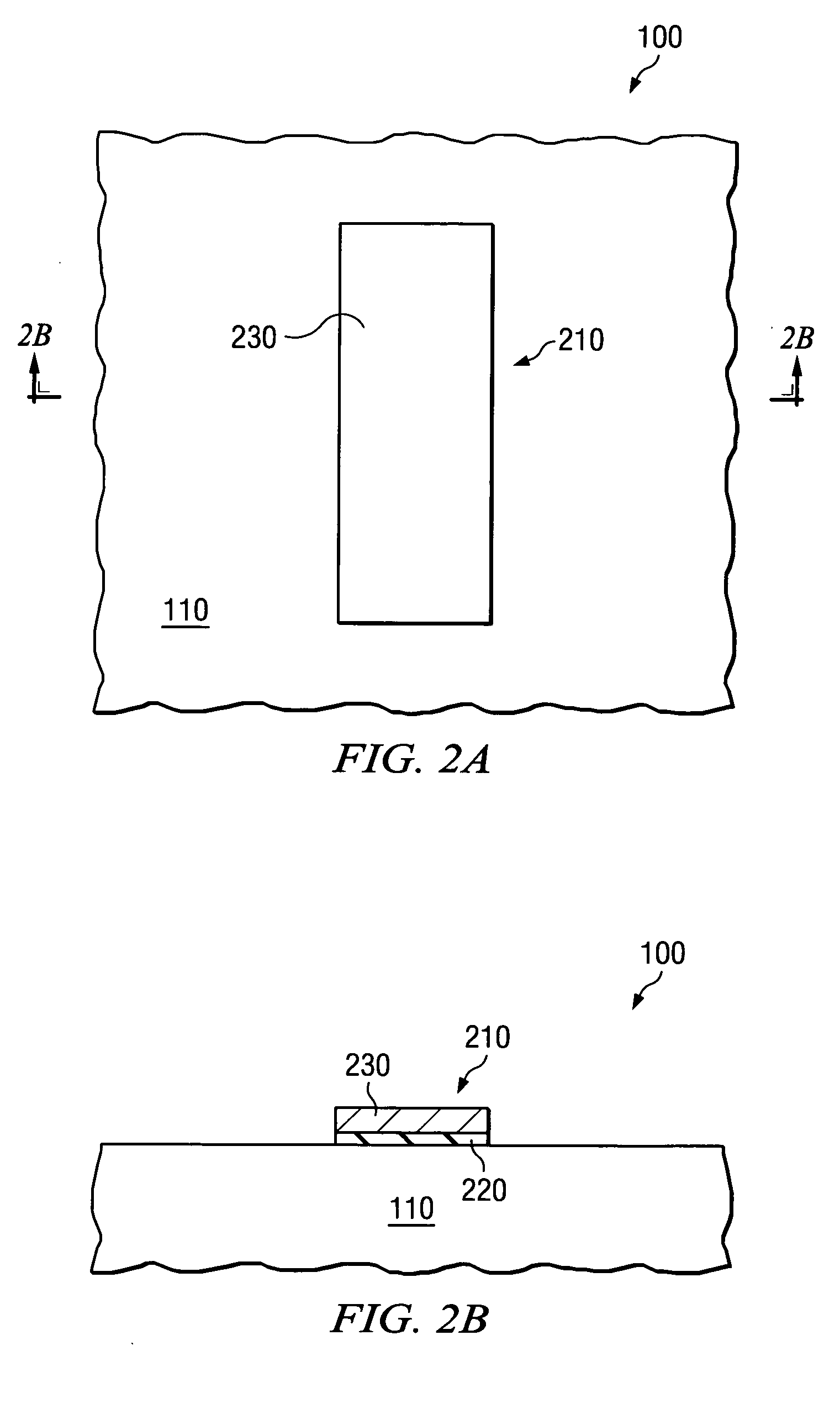
[0028] In the following FIGUREs, a sectional view of a transistor device 100 fabricated according to the principles is presented. When the goal of clarity is served, a plan view is also shown, including outlines of underlying structures to clarify the positional relationships of the elements of the transistor device 100 during manufacture. Furthermore, an additional sectional view taken at another position on the transistor device 100 may also be presented when appropriate.

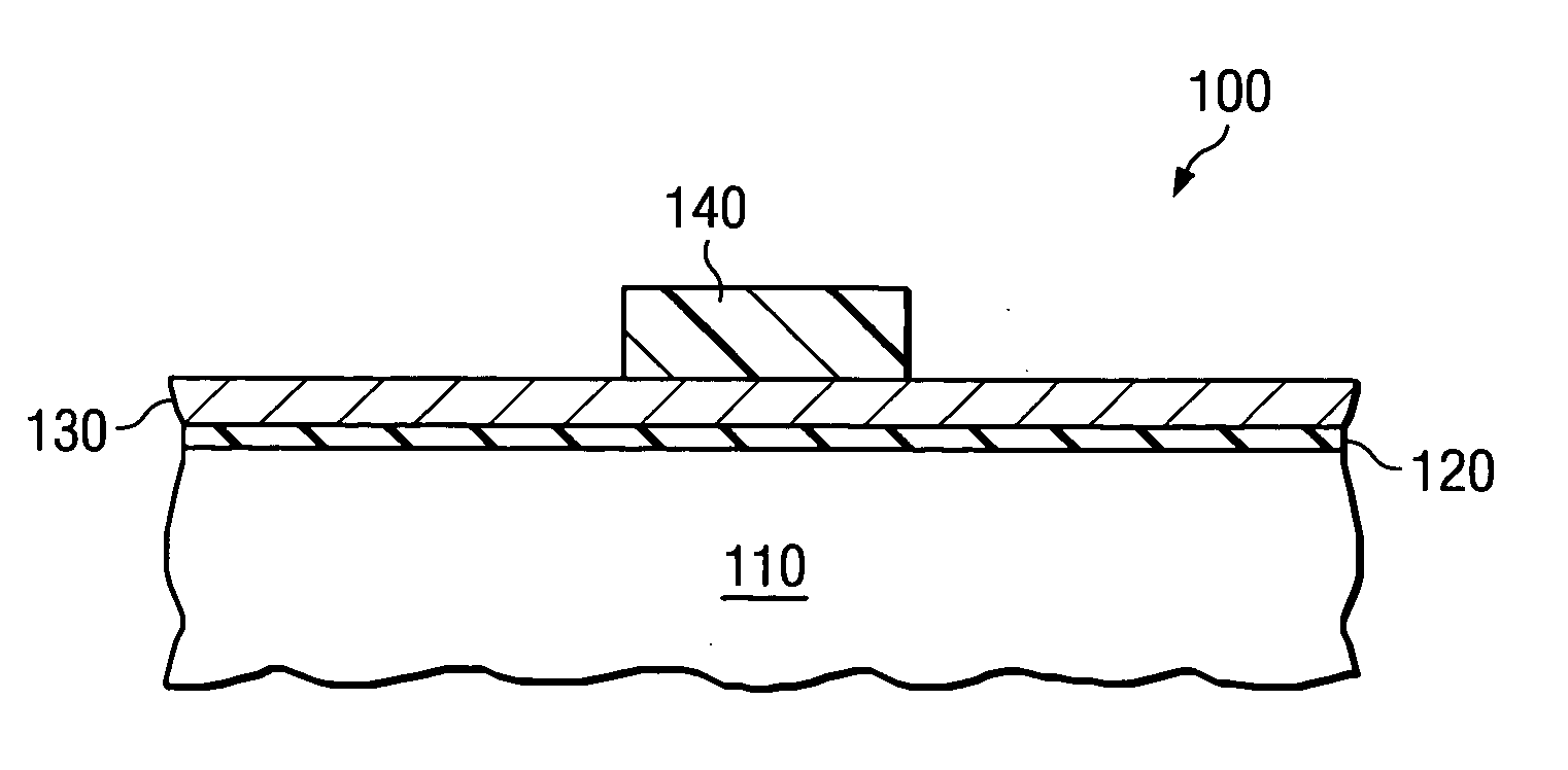
[0029] Referring initially to FIGS. 1A and 1B, illustrated are a plan view and a sectional view, respectively, of a partially completed transistor device 100 fabricated according to the principles of the invention. The transistor device 100 is fabricated on a substrate 110. The substrate 110 may be a conventional semiconductor, and may further be a semiconductor wafer suitable for semiconductor device manufacturing. An example of such a wafer is a 200 mm or 300 mm silicon wafer. Those skilled in the art will appr...


PUM


Abstract

The present invention provides a method of manufacturing a transistor device, a transistor device, and a method for manufacturing an integrated circuit. In one aspect, the method of manufacturing a transistor device includes providing a gate structure (140) over a substrate (110). An insulating layer (310) is formed over the gate structure (140), and openings (710) to the substrate (110) are formed therein, thereby removing a portion of the gate structure (140). The openings (710) are filled with a conductor (1410), thereby forming an interconnect (1510).

Description

TECHNICAL FIELD OF THE INVENTION [0001] The present invention is directed, in general, to a method of forming a transistor device, and in particular, a method of forming a transistor device in which contacts to the transistor are self-aligned to the transistor gate. BACKGROUND OF THE INVENTION [0002] The trend in semiconductor technology to double the functional complexity of its products every 18 months (Moore's “law”), which is still valid today after having dominated the industry for the last three decades, has several implicit consequences. First, the cost per functional unit should drop with each generation of complexity so that the cost of the product with its doubled functionality would increase only slightly. Second, the higher product complexity should largely be achieved by shrinking the feature sizes of the chip components while holding the package dimensions constant; preferably, even the packages should shrink. Third, the increased functional complexity should be parall...

Claims


Application Information

Patent Timeline
IPC IPC(8): H01L21/3205
CPCH01L21/76813H01L21/76831H01L21/76895H01L21/76897H01L2924/0002H01L29/66492H01L2924/00
Inventor MARSHALL, ANDREWGELSOMINI, TITODAVIS, HARVEY EDD
Owner TEXAS INSTR INC
Learn More