

Pixel having two semiconductor layers, image sensor including the pixel, and image processing system including the image sensor
a technology of image sensor and semiconductor layer, applied in the field of image sensor pixels, can solve the problems of increasing production cost, limiting the “megapixel” capacity and color sensitivity of image sensor, and limiting the image quality of images captured by digital cameras
- Summary
- Abstract
- Description
- Claims
- Application Information
AI Technical Summary
Benefits of technology
Problems solved by technology
Method used
Image

Examples
Embodiment Construction
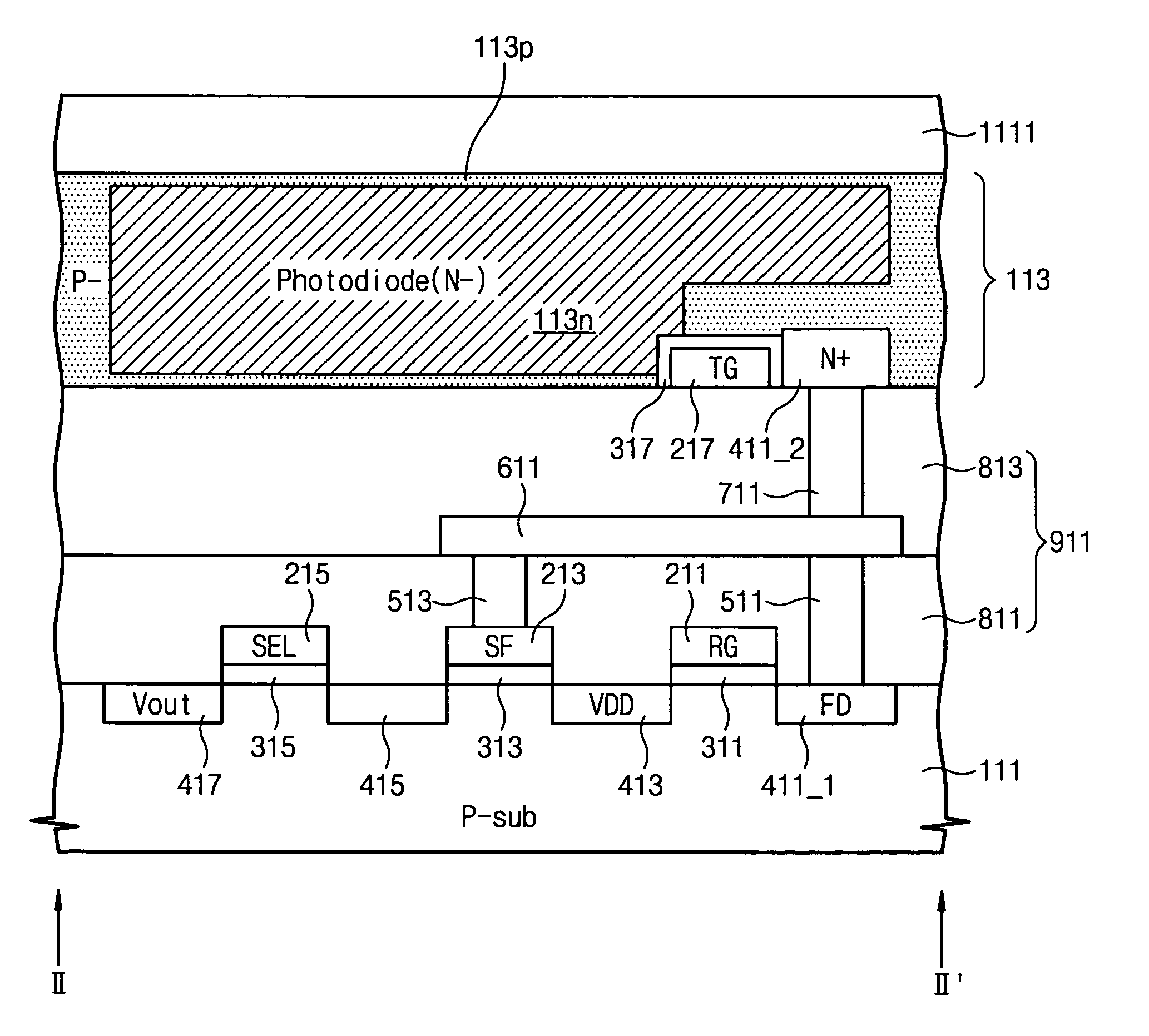
[0042]FIG. 3 is a perspective view of a pixel in an image sensor in accordance with an embodiment of the invention. Referring to FIG. 3, a pixel 101 according to the embodiment by the invention comprises a photodiode 115, and transfer, reset, source follower, and selection transistors operationally coupled with the photodiode 115. According to this embodiment of the invention, the components of the pixel 101 are arranged in separate first and second semiconductor patterns 111 and 113 that are spaced apart from each other. In this exemplary embodiment of the invention, the photodiode 115 and the transfer transistor are disposed in the second semiconductor pattern 113, while the reset, source follower, and selection transistors are placed in the first semiconductor pattern 111. The gate 217 of the transfer transistor is disposed under the photodiode 115. Thus, the fill factor of the pixel is not affected by the presence or size of the transfer, reset, source follower, and selection tr...
PUM
 Abstract
Description
Claims
Application Information